
Digital sine wave generator

The circuit design described integrates several key components to achieve a sine wave output through a systematic approach. The reverse binary counter D2 is responsible for counting in reverse, which is crucial for generating the desired waveform. The binary-coded decimal decoder D3 decodes the counter's output into a format that can trigger the logic gates, specifically D1.3 and D1.4. These gates function as a control mechanism, switching the operational mode of the counter based on specific output conditions.
The resistors R1 to R9 play a vital role in shaping the initial quarter of the sine wave, ensuring that the output signal begins accurately. The summing operational amplifier A1 is central to the process, as it combines the outputs from the resistors to create the positive half of the sine wave. The subsequent negative half-wave is achieved through the use of amplifier A2, which alternates its configuration based on the timing of the input cycles, effectively ensuring that the waveform is continuous and smooth.
The gain control provided by FET transistor V4 is an essential feature, allowing for dynamic adjustment of the output signal's amplitude. The circuit's feedback mechanism, which includes the level shifting transistors V1 and V2, ensures that the signal remains within acceptable voltage ranges, thereby preventing distortion and maintaining fidelity in the output waveform.
The use of a potentiometer R13 for fine-tuning the output voltage further enhances the circuit's usability, enabling precise adjustments to achieve the desired output characteristics. This comprehensive design allows for the effective generation of sine wave signals suitable for various applications in electronic systems.By using the reverse binary counter and the binary-coded decimal decoder can obtained the step voltage, and by approximating this voltage can be produced the sine wave signal with sufficient accuracy, suitable for many purposes. In the circuit diagram of the digital generator (see figure 1) the resistors R1. R9 is used to produce the first quarter of the sine wave (while the reverse counter D2 has normal counting mode) as the current, applied to the inverting input of the summing operational amplifier A1. The trigger, composed of the two logic gates D1. 3 and D1. 4 will be switched when the outputs "0" or "9" of the decoder D3 changes to logic zero, this trigger controls the mode (reverse or normal) of the reverse counter.
Thus, for twenty clock ticks at the input of the generator, the output of the summing amplifier A1 will create the positive half-wave sine wave. The negative half-wave will be formed within the next twenty cycles by inverting the positive half-wave with the amplifier A2, which operates alternately (the first 20 cycles the amplifier A2 works as the non inverter, the next 20 cycles it works as the inverter).
The gain of the amplifier switches by the FET transistor V4 from -1 to +1. The signal from the output of RS flip-flop (D1. 3, D1. 4) feeds through the D flip-flop D6 and the zener diode V1 to the transistors V1 and V2 (level shifting circuit) and further on the gate of the FET transistor V4. The voltage taken from the wiper of potentiometer R13, is adjusted to get zero voltage at output of the summing amplifier A1 while all outputs of the counter D2 has logic zero.
🔗 External reference
Related Circuits
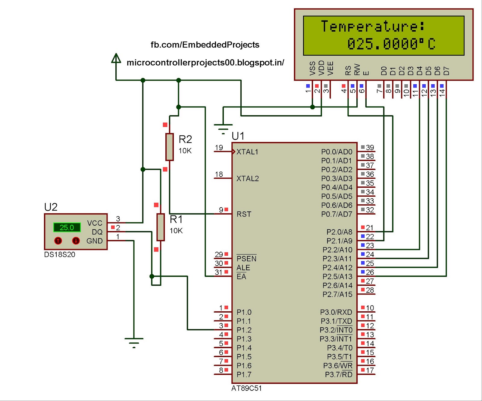
The hardware configuration for utilizing multiple 1-Wire temperature sensors, such as the DS1820, is straightforward. Communication between the microcontroller and the temperature sensors occurs over a single-wire bus, which can also supply power to the devices. An extensive number...
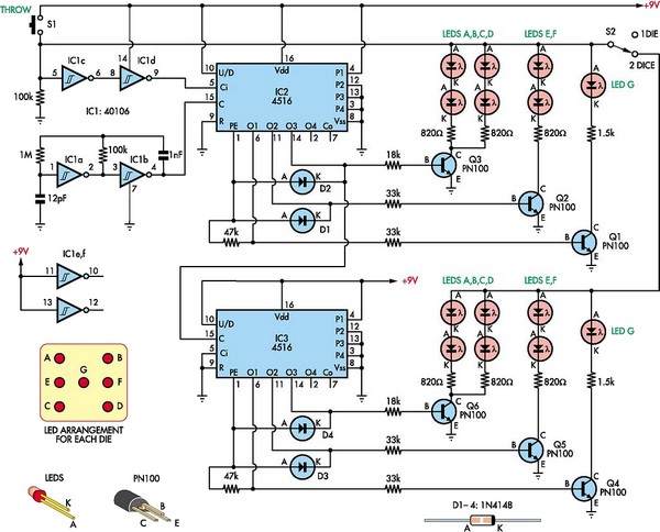
This circuit utilizes two 4516 integrated circuits (ICs) to simulate a game involving two dice. A switch is included to select whether one or two dice will be activated with each press. A 9-volt battery is sufficient for power...
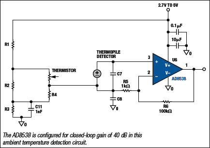
Due to their speed, accuracy, effectiveness, and cost-efficiency, infrared (IR) digital thermometers have supplanted traditional mercury thermometers. An ear digital thermometer utilizes a thermopile sensor to measure the infrared heat emitted by the eardrum, which correlates with the temperature...
With the increasing awareness of environmental issues and the energy crisis, the development and utilization of new energy sources have garnered more attention. Solar energy has recently become popular due to its inexhaustible, efficient, and pollution-free characteristics. The photovoltaic...

This circuit generates a wide variety of noise types, including white noise, pink noise, high pass noise, grainy noise (with adjustable graininess), and adjustable random gates. It is designed for enthusiasts of noise generation. The noise source is derived...
The digital thermometer consists of a temperature sensor, a single stabilizing circuit, a counter circuit, a decoding section, a driving circuit, and LED digital tubes among other components. It operates within a temperature range of 0 to 50 degrees...