
Discrete components stereo encoder circuit diagram

The debugging process involves connecting the FM modulator to a five-volt power supply and measuring each pin of IC1 (CD4069) and IC2 (CP, Q) with a multimeter, ensuring that each pin reads half of the supply voltage, indicating proper oscillator startup. A digital frequency meter can be used to measure the output frequency of IC1, which can be adjusted to 75 kHz +/- 10 Hz using potentiometer RW1. If the frequency is not aligned, the radio can be tuned using RW2, followed by RW1, to ensure the radio's stereo indicator lights up without frequency howling from the speaker. The circuit accepts a stereo audio signal (1.5 Vpp) from the input terminal, allowing reception of stereo broadcasts on the radio. The input signal can alternatively be sourced from a line, necessitating an adjustment to resistor R7. Additionally, high-frequency noise can be minimized by adjusting R7, which, along with R6, serves as external components equivalent to pins 13-14 of the BA1404, facilitating the mixing of the pilot signal and composite signal before amplification. The circuit, utilizing the 9014 and BA1404, enters from pin 12, and there are numerous opportunities for improvements and developmental enhancements within this design. Circuit schematic diagram IC1-4069 the Y1, Y2 to form a frequency 76KHZ oscillator, Y3-Y6 isolation after shaping into the IC2 CD4027 dual JK flip-flop consisting of two compon ent frequency circuit that generates a symmetric +/- 38KHZ and 19KHZ square wave, square wave +/- 38KHZ which is used to control the analog switch IC3 CD4066, after stereo input audio signal switching with a frequency-modulated signal 19KHZ and then mixed into isolation after the transistor 9014 FM modulator. FM modulator circuit can be found in the site in a variety of FM transmitter circuits. This article is not shown, the purpose is to let the fans can easily use this encoder, not only can increase the functionality of your old stereo FM transmitter, but also as a general-purpose equipment.
Debugging is connected as the FM modulator and a five-volt power supply, measured with a multimeter IC1CD4069 each foot and IC2 CP, Q, Q, each foot should be half the supply voltage has been described oscillator start-up. If a digital frequency meter, measuring IC1 output frequency, the frequency is adjusted RW1 75KHZ +/- 10HZ can.
If not, can be aligned radio, RW2 half after a good tune, and then transferred RW1, make radio stereo indicator light, and the speaker is no temple frequency howling. And then into the stereo audio signal (1.5Vpp, available power amplifier output) from the input terminal at this time you will be able to receive stereo broadcasts on the radio.
The input signal can also be obtained from the line, but this time R7 should be changed accordingly. Finally, you can also adjust the high-frequency noise R7 minimum, in fact, R6, R7 is equivalent to BA1404 of 13-14 feet in external components, is a pilot signal and a composite signal mixing circuit and input to the amplifier, this circuit is 9014, and BA1404 in from 12 feet on entering, I think this circuit there are many places for improvement, development of what it might be interested in.
Related Circuits
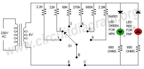
This is a simple transistor tester circuit that can be utilized to test both NPN and PNP transistors. The voltage source consists of a 6V power supply, which is derived from a step-down transformer that converts 230V AC to...

The circuit utilizes a motor auto-voltage transformer for starting. The motor auto-voltage transformer start circuit is designed to provide a controlled method for initiating the operation of an electric motor. This type of circuit is particularly beneficial in applications where...

A XICOR X9241 POT IC module can be utilized to modify the four digital analog circuits, as depicted in the schematic. The XICOR X9241 is a digital potentiometer integrated circuit designed for precise adjustment of analog signal levels in various...

Do you long for a beach holiday on a tropical island, but you don't have the necessary means? There is a solution: build the i-TRIXX surf simulator, put on your headphones, and escape from this mundane reality. Allow the...
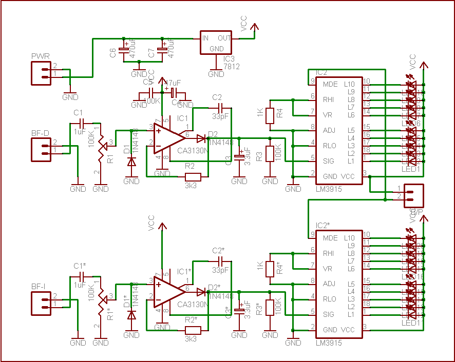
This simple circuit is based on the well-known integrated circuit LM3915. The main characteristic of this integrated circuit is its ability to manage 10 Light Emitting Diodes (LEDs) in a logarithmic scale, with a 3dB difference between the LEDs,...
The circuit below demonstrates the generation of a single positive pulse that is delayed in relation to the trigger input time. It is similar to a previously described circuit but utilizes two stages, allowing for control over both the...