
Generating a Delayed Pulse Using The 555 Timer circuit
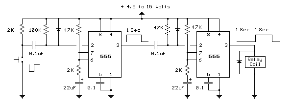
The circuit employs two 555 timer ICs configured in monostable mode to achieve the desired pulse generation and delay. The first 555 timer is triggered by a momentary push-button switch, which, when pressed, causes the output to transition high, activating the relay. The output remains high for a predetermined duration, set by an external resistor and capacitor connected to the timing pins of the first 555 timer. This timing component determines the length of the delay before the output transitions back to low.
Once the output of the first timer returns to low after the delay, this falling edge is fed into the trigger pin of the second 555 timer. The second timer is also configured in monostable mode, and it is designed to produce a pulse of a specified width. Its timing components (resistor and capacitor) set the duration of this pulse. The output of the second timer, which drives the relay, remains high for the duration of this pulse, allowing the relay to energize briefly before returning to a de-energized state.
The integration of two stages provides flexibility in controlling both the delay and the pulse width, making this circuit suitable for applications requiring precise timing sequences. The use of a dual 555 timer (556) can simplify the circuit design, reducing the number of components needed while maintaining the same functionality. However, care must be taken to reference the correct pin configurations when using the 556 timer, as they differ from the standard 555 timer layout.The circuit below illustrates generating a single positive pulse which is delayed relative to the trigger input time. The circuit is similar to the one above but employs two stages so that both the pulse width and delay can be controlled.
When the button is depressed, the output of the first stage will move up and remain near the supply voltage un til the delay time has elapsed, which in this case is about 1 second. The second 555 stage will not respond to the rising voltage since it requires a negative, falling voltage at pin 2, and so the second stage output remains low and the relay remains de-energized. At the end of the delay time, the output of the first stage returns to a low level, and the falling voltage causes the second stage to begin it`s output cycle which is also about 1 second as shown.
This same circuit can be built using the dual 555 timer which is a 556, however the pin numbers will be different. 🔗 External reference
Related Circuits
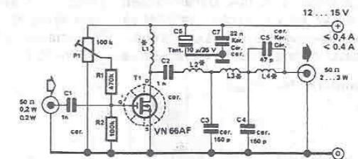
By using this RF amplifier, small power transmitters of 200 mW can be upgraded to reasonable power transmitters, ranging between 2 and 3 W. The circuit is straightforward. The output filter network suppresses noise by at least 55 dB....
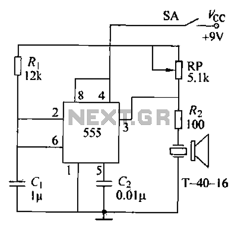
The circuit comprises an ultrasonic transmitter and a T-4 0-16 555 timer circuit. By adjusting the potentiometer RP, the frequency of the oscillation circuit can be modified. The circuit emits ultrasonic signals at a frequency of 40 kHz, with...
The circuit is illustrated in Figures 16-95 to 16-97. The electrode automatic adjuster demonstrates enhanced performance, featuring a high-accuracy, well-linear current output type bridge. Additionally, it incorporates a differential arc current negative feedback circuit (advanced) that allows for preemptive...

The UCD90124/A is utilized to monitor multiple voltages, some of which exceed 2.5V. Scaling circuits are implemented to prevent exceeding the 2.5V maximum on the MON inputs. The inquiry pertains to whether raw voltage values or scaled values should...
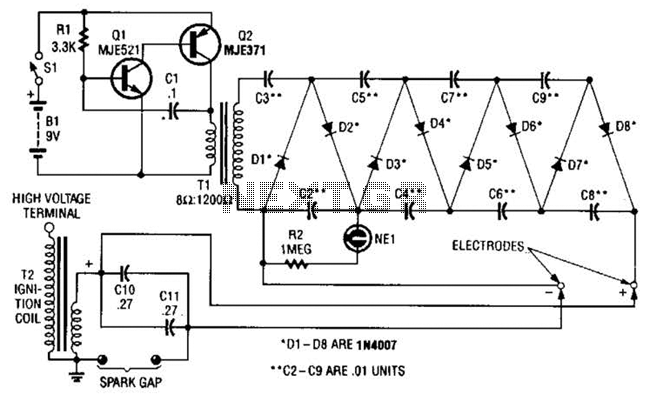
This circuit employs a transistor oscillator and a voltage multiplier to charge capacitors CIO and CI1 to a high voltage. When the spark gap breaks down, T2 generates a high-voltage pulse through the discharge of capacitors CIO and CI1...
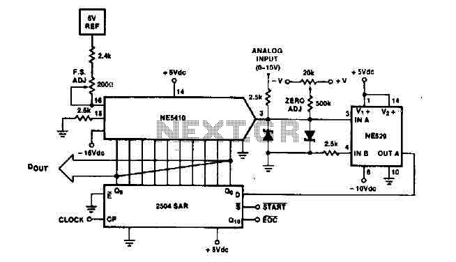
The time IO-bit conversion operates at 3.3 MHz with a clock signal. This converter utilizes a 2504 12-bit register in successive approximation mode, where the conversion signal for the short-cycle end is derived from the first bit utilized in...