
Dual 25W stereo audio power amplifier circuit
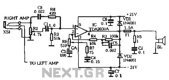
The Lisheng power amplifier circuit is designed to deliver high-fidelity audio output while maintaining stability and reliability. The use of a high-pass filter ensures that only the desired audio frequencies are amplified, preventing low-frequency noise from interfering with the performance of the amplifier. The feedback loop plays a crucial role in shaping the amplifier's frequency response, allowing for tailored adjustments to the audio output.
The treble and bass boost circuits are particularly significant for achieving a rich audio experience, allowing the user to customize the listening experience based on personal preferences. The careful selection of component values, such as the capacitors and resistors, is essential for achieving the desired frequency response and ensuring that the amplifier operates within optimal parameters.
Furthermore, the inclusion of protection diodes enhances the longevity of the amplifier, making it robust against unexpected surges or faults. The overall design reflects a comprehensive understanding of audio amplification principles, ensuring that the circuit not only meets performance expectations but also provides a user-friendly experience.The entire circuit consists of two parts - Lisheng power amplifier and the rectifier filter crossing. As shown in Figure 5-85 is a stereo audio power amplifier circuit diagram t figure depicts only one channel, the other channel with this identical. The audio signal is applied to the XS1 4. 7k, 0 volume potentiometer RP2, and then by the ci, Rl away amplifier IC TDA2030A o cl, Rl to form a high-pass filter circuit, first as an audio signal through an intersection, it this value is crucial pregnant Cl was taken 0.1V: F, Ri taken 51k, fl, to ensure the above evidence ZOHz VLF signal destructive consumption ^ IC inlet port to the Further, the feedback loop R 6, C3 is the entire circuit affect the frequency response of a cross key point here C3 use 10Q ~ 220vF tantalum capacitors, and R6 so low corner frequency 3Hz hereinafter are for the same consideration o R4, R6. C3 composed negative feedback loop, R4 and R6 the ratio determines the gain of the circuit, the specific value by the formula f ,, - 1 + R4 / R6 wherein R6 fork and obtained export R7 and C4 form a treble boosting circuit to enhance the frequency of about 3.
3kHz - 16kHz, about promotion is 15dB, increase transparency playback Ca 6 R3, R4 and C5 bass boost circuit, lifting frequency 20 ~ 200Hz, focusing on ultra-low-frequency band, the maximum lift capacity of up to 20dB, for enhancing the strength and feeling in playback b appropriate to enhance the bass sound during playback, not only can improve tone Tan t also insufficient balance loudness entire band t fit everyone's listening habits. R5 and C2 form Joubert network, the transition frequency of about 160kHz, the connection with the speaker system from 20kHz above come into play, attenuating high frequency signals to prevent UHF since the withdrawal o C6 C7 back to power + decoupling capacitors to eliminate the interference noise power, greatly improve the transient response of the power supply.
VD1, VD2 for protecting the integrated amplifier circuit TDA2030A, when the circuit is working properly when they do not work, but the circuit is unexpected, it was to protect the IC from the port because a crucial role for the sake of improving reliable circuit, VD1 , VD2 is better fitted to the mouth c8.R8 and RZ form a high-frequency compensation network, with loudness control features, can improve the small volume playback quality mouth
Related Circuits
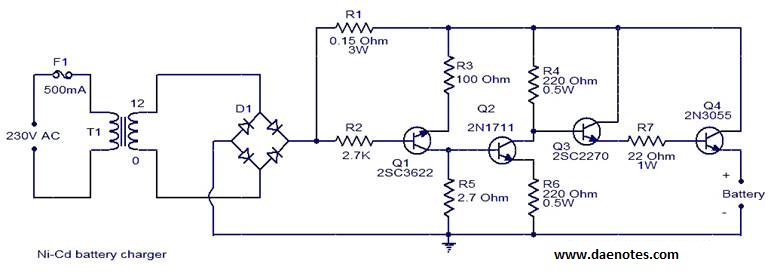
This circuit is primarily designed for charging 12V Ni-Cd battery packs. However, it can also be used to charge 6V and 9V battery packs with slight modifications. The circuit operates by utilizing a power supply that provides the necessary voltage...
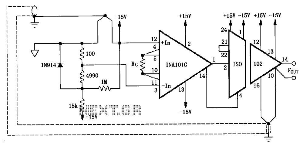
The circuit, as illustrated in the figure, consists of an ISO102 and an INA101 designed to eliminate ground loops and provide high-end cold junction compensation for a thermocouple amplifier. This configuration utilizes a K-type thermocouple to detect temperature at...
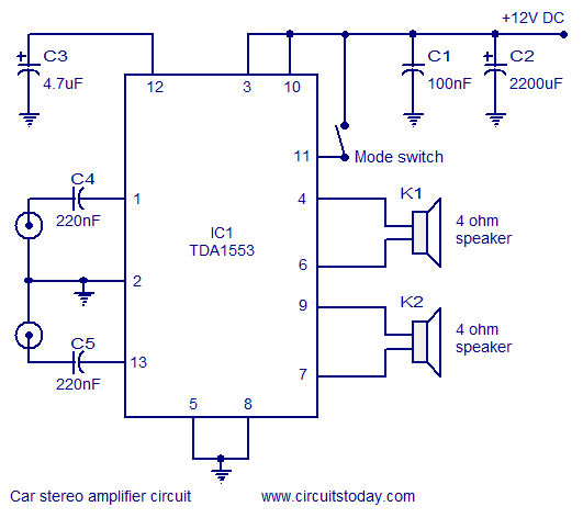
A car stereo amplifier circuit that can be used in automobiles, designed using the Class-B audio amplifier TDA1553, complete with a circuit diagram and schematics. The car stereo amplifier circuit utilizes the TDA1553, a Class-B audio amplifier known for its...
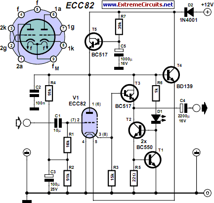
Headphone listening can be technically superior as it eliminates room reflections, and the close contact between the transducer and the ear requires only minimal power. This small power requirement allows transducers to operate at a fraction of their full...
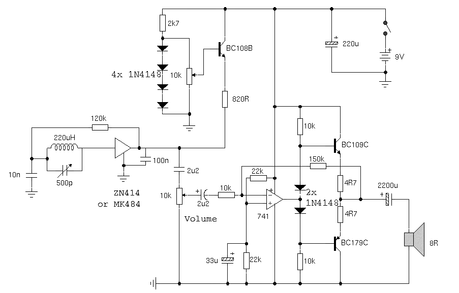
The circuit demonstrates the application of the ZN414 integrated circuit (IC) to create a compact AM radio receiver. The ZN414 IC is a combination of a transistor and a tuned radio frequency (TRF) circuit. The ZN414 IC is specifically designed...
This schematic is directly sourced from the Altera ByteBlaster datasheet or manual, which provides comprehensive details regarding the connector's functionality and pin connections. It is advisable to review the datasheet available on their website or through a search engine...
Warning: include(partials/cookie-banner.php): Failed to open stream: Permission denied in /var/www/html/nextgr/view-circuit.php on line 713
Warning: include(): Failed opening 'partials/cookie-banner.php' for inclusion (include_path='.:/usr/share/php') in /var/www/html/nextgr/view-circuit.php on line 713