
Efficient Power Booster
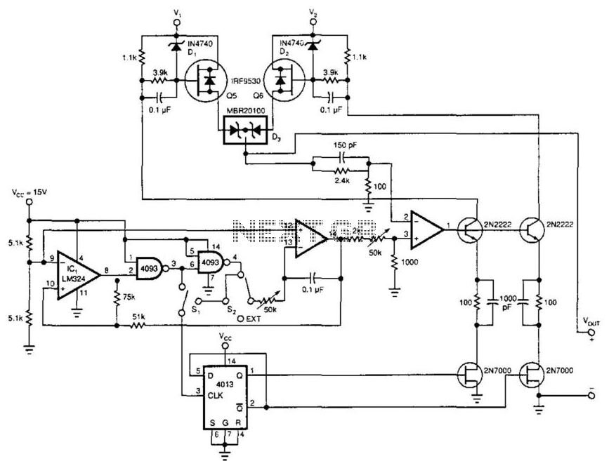
This circuit design incorporates a power booster that can operate in two distinct modes: as a power multiplexer and as a linear amplifier. In multiplexer mode, the circuit effectively utilizes two power sources, VI and V2, allowing for alternating power delivery to the load. This method benefits from reduced power dissipation due to the switching nature of the power-handling devices, which operate in a manner akin to digital switches.
The timing characteristics of the circuit are governed by the RC time constant associated with the integrator, IC1. This time constant is critical as it directly influences the oscillation frequency of the circuit, thus impacting the performance when generating high-power square wave outputs. When an external drive signal is introduced, the circuit transitions to linear amplifier mode, where it amplifies the input signal while managing power dissipation more variably. The design ensures stability at gains exceeding 15, which is essential for maintaining signal integrity and performance across a range of applications.
Protection mechanisms are integral to the design. Diodes D1 and D2 are strategically placed to limit the gate voltage swing of the FETs, ensuring that it does not exceed 15 V, thereby preventing potential damage to the FETs. Additionally, D3, a dual Schottky diode, plays a critical role in protecting the FETs from unintended short circuits that may occur between the two power supplies due to the parasitic properties of the FETs. This feature enhances the reliability of the circuit under varying operational conditions.
For applications requiring high-frequency switching, such as driving the FETs Q5 and Q6 at frequencies greater than 1 kHz, the inclusion of gate drivers is necessary. These drivers provide the necessary voltage and current to switch the FETs effectively, ensuring optimal performance and response times in high-speed applications. Overall, this power booster circuit is designed to deliver high efficiency and versatility for various electronic applications, from power multiplexing to linear amplification. This power booster functions as a high-efficiency "power multiplexer" or, if you supply an external signal-source, as a high-power linear amplifier. If you want to drive a load with a high-power square wave, the circuit simply draws power from two external power sources, VI and V2, alternately. In this mode, the circuit"s power-handling devices function as switches, dissipating minimal power. The RC time constant of the integrator, IC1, determines the circuit"s oscillation period. If you supply an external drive waveform, the circuit functions as a linear amplifier, and, consequently, inherently dissipates varying portions of that power.
The power amplifier is stable for gains > 15. Diodes D1 and D2 limit the FET"s gate-voltage swing to less than 15 V. D3 is a dual Schottky diode that protects the FETs from short circuits between the two supplies, VI and V2, through a FET"s parasitic diode. With D3 in place, you can choose either power channel for the higher voltage input, lb drive the FETs, Q5 and Q6, at switching frequencies greater than 1 kHz, you will have to use gate drivers for them.
🔗 External reference
Related Circuits
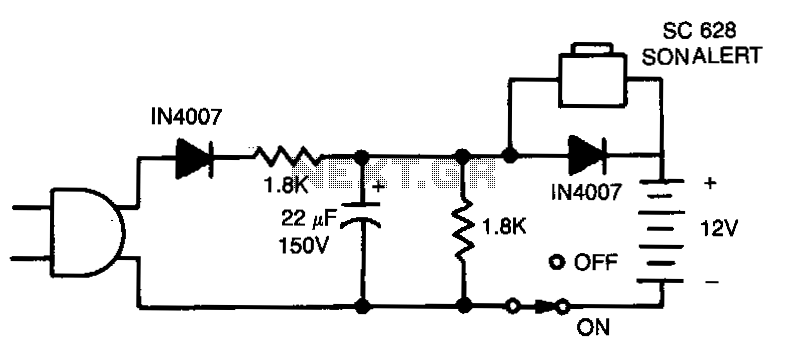
When the power is turned off, the alarm activates when switch S1 is closed. The 12-V battery remains charged when the circuit is connected and the switch is in the "on" position. The described circuit features an alarm system that...

Power supply for a 25W power amplifier based on a MOSFET design. This power supply circuit is paired with a high-power audio amplifier rated at 1500 watts. The design of the power supply for the amplifier requires careful consideration....
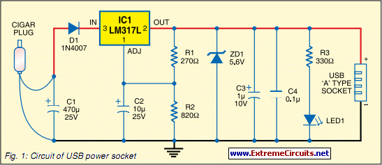
Today, nearly all computers are equipped with logic blocks designed to implement a USB port. In practice, a USB port can deliver over 100 mA of continuous current at 5V to the peripherals connected to the bus. This capability...
This small and compact stereo amplifier is powerful and can easily replace a broken amplifier or be used in new constructions, or to create an active speaker, when combined with a preamplifier. Its remarkable features make it a true...
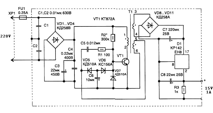
A 15 Watt switching power supply schematic diagram features a pulse transformer T1 constructed on a ferrite core M2500NMS-2 or M2000NM9, with a Sh5h5 size (cross-section of the magnetic coils at the location of 5G—5 mm with a gap...
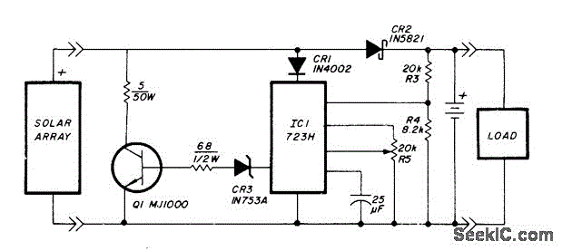
A voltage regulator is connected across the solar cell to prevent damage to the storage battery due to overcharging. A series diode prevents the array from discharging the battery during hours of darkness. The regulator does not draw power...