
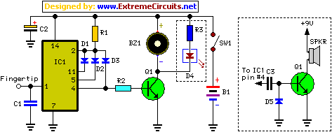
Electronic 7-Digit Combination Lock

The 7-digit combination lock circuit is designed for reliable operation and ease of use. The heart of the system is the 4-bit Johnson counter (IC1), which counts the number of valid button presses in a predetermined sequence. The ten push button switches are strategically arranged to allow the user to input the combination. Each switch corresponds to a specific output of the counter, facilitating the lock mechanism's activation when the correct sequence is entered.
The reset mechanism is crucial for ensuring the security of the lock. Capacitor C2's charging through the 820-kilo-ohm resistor establishes a stable initial state. When a button is pressed, the discharge of C2 through diode D1 and resistor R2 allows the counter to exit the reset state, enabling it to begin counting valid inputs. The filtering action of capacitor C1 and resistor R3 is essential to prevent false triggering due to mechanical bounce when the buttons are pressed, ensuring that each press is registered as a single event.
The output logic of the counter is designed to provide a clear indication of the current state. As each button is pressed in the correct order, the corresponding output transitions from high to low, allowing the system to track progress through the combination sequence. If the sequence is interrupted or if the time between presses exceeds the threshold defined by C1's charging time, the counter resets, enhancing security.
Upon successful entry of the complete sequence, output O7 activates for a duration of approximately ten seconds, providing ample time for the solenoid valve to actuate and unlock the mechanism. The use of a driver transistor (T2) ensures that the solenoid receives adequate current to operate effectively, further enhancing the system's reliability.
The physical assembly of the circuit on a PCB should be done with care to avoid shorts, and the use of an IC base allows for easy replacement and troubleshooting of the counter IC. The enclosure in a plastic cabinet not only protects the components but also provides a user-friendly interface with the switches positioned conveniently for operation. This combination lock circuit exemplifies a practical application of digital logic and electronic components in security technology.This 7-digit combination lock can be easily hard-wired for any combination that you choose. The circuit uses a 4-bit, divide-by-8 Johnson counter (IC1), ten push button switches and NPN transistor T1. At power-on, ` capacitor C2 connected to pin 15 of IC1 charges to high level through 820-kilo-ohm resistor, holding the counter in the reset state.
I n this condition, output O0 (pin 2) of counter IC1 is high, while all other outputs are low. When switch S2 is pressed, transistor T1 conducts and capacitor C2 discharges via diode D1 and resistor R2, releasing the counter`s reset input. When S2 is released, T1 cuts off and its collector is pulled high, generating a rising edge on the counter`s input clock pin 14.
Capacitor C1 and resistor R3 in the base circuit of transistor T1 form a simple filter to prevent switch contact bounce from generating multiple clock pulses on pin 14 of IC1. The clock pulse advances IC1`s count by one, so O0 goes low and O1 goes high. Therefore press switch S7 next, as it`s wired to output O1. The time required for capacitor C1 to charge to logic high level is the maximum time that can lapse between switches pressed.
Otherwise, the counter will reset. When all switches have been pressed in the correct sequence (S2-S7-S3-S4-S5-S2-S2 as shown), output O7 (pin 10) of the counter goes high for about ten seconds. This output is fed to driver transistor T2 to drive the solenoid valve and open the lock. Assemble the circuit on a common PCB and enclose in a plastic cabinet. Connect the solenoid valve to the circuit using a flexible wire. While soldering, take care to avoid shortings. Use IC base for ease of troubleshooting. Connect the switches for opening the lock at the top of the plastic case. 🔗 External reference
Related Circuits
A Super GameBoy was acquired, but it has been observed that the sound pitch is significantly higher than that of an original GameBoy. This discrepancy arises due to a mismatch in CPU clock frequencies: 4.194304 MHz for the original...
This precise one-pulse-per-second clock is constructed using a few common components and is driven by a 50 or 60 Hertz mains supply, without any direct connection to it. It produces a beep or metronome-like click and/or a visible flash...
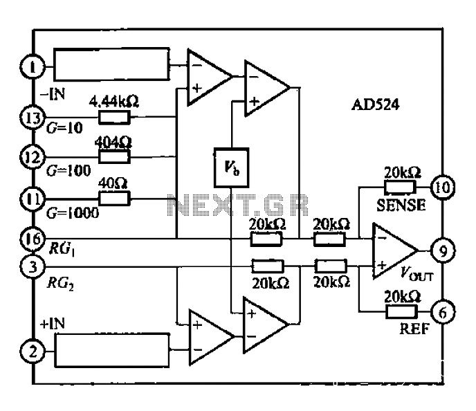
The AD524 is a low-drift instrumentation amplifier characterized by a drift voltage of 0.5 mV and a maximum drift of 25 mV at room temperature. It has low noise performance with a noise level of 0.3 mVp-p in the...
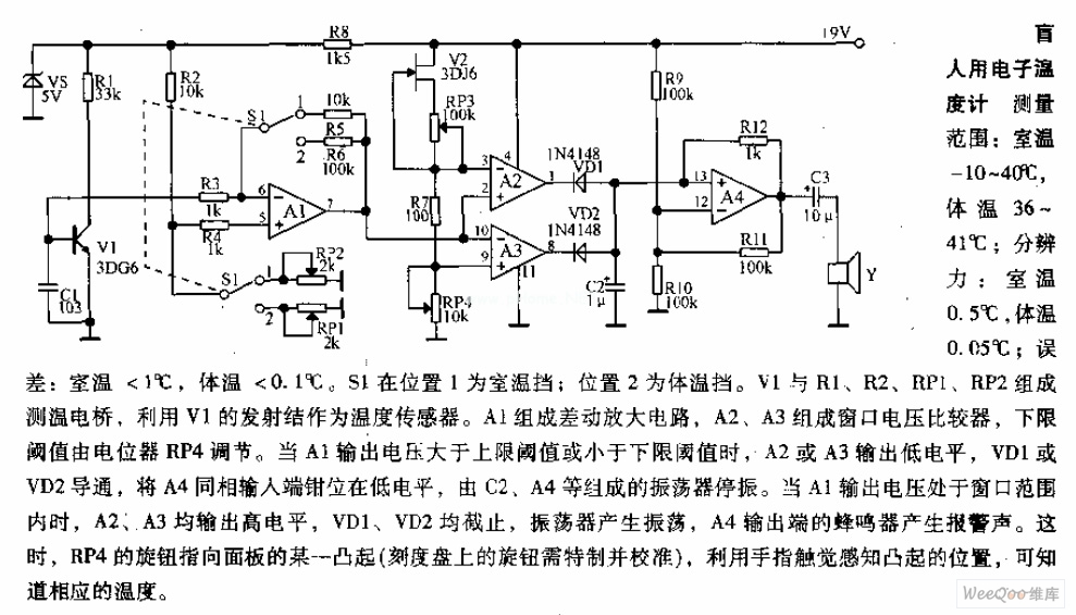
Measuring range: room temperature is -10 to 40 degrees Celsius; body temperature is 36 to 41 degrees Celsius; Resolution: room temperature is 0.5 degrees Celsius, body temperature is 0.05 degrees Celsius; error: room temperature <1 degree Celsius, body temperature <0.1 degrees Celsius. When switch S1 is in position 1, it displays the room temperature profile; position 2 displays the body temperature profile. Components V1, R1, R2, RP1, and RP2 form the temperature measurement circuit. The temperature measurement circuit is designed to monitor and display two distinct temperature ranges: ambient room temperature and body temperature. The circuit operates with a measuring range for room temperature from -10 to 40 degrees Celsius and for body temperature from 36 to 41 degrees Celsius. The resolution of the circuit is fine-tuned to provide accurate readings, with a room temperature resolution of 0.5 degrees Celsius and a body temperature resolution of 0.05 degrees Celsius. The specified error margins indicate a maximum deviation of less than 1 degree Celsius for room temperature measurements and less than 0.1 degrees Celsius for body temperature measurements. The circuit utilizes a switch, S1, which allows the user to select between the two temperature profiles. In position 1, the circuit outputs the room temperature, while in position 2, it outputs the body temperature. The operational components include a voltage source (V1), resistors (R1, R2), and potentiometers (RP1, RP2) that are integral to the measurement process. Resistors R1 and R2 are likely part of a voltage divider network that aids in scaling the temperature sensor output to a readable format. Potentiometers RP1 and RP2 can be used for calibration purposes, allowing fine adjustments to ensure that the readings are accurate within the specified error margins. The temperature sensor, which is not explicitly mentioned but is assumed to be part of the circuit, converts temperature changes into an electrical signal that can be processed by the circuit. The output from the sensor is conditioned by the resistive components to produce a voltage level that corresponds directly to the measured temperature. This voltage is then displayed on an appropriate display unit, which could be an analog gauge or a digital readout, depending on the design of the circuit. Overall, this temperature measurement circuit is a practical solution for monitoring both ambient and body temperatures with high accuracy and user-friendly operation through the selection switch.
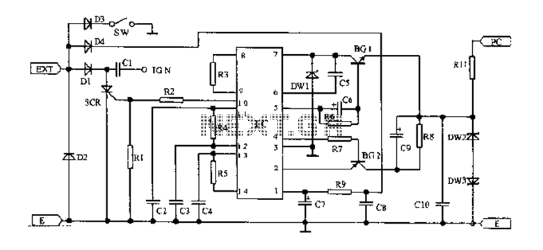
An AC magneto is connected to an external circuit. The output is rectified by diode D1 and stored in capacitor C1. Additional rectification is performed by diodes D4, along with resistors R9 and capacitors C7 and C8, which filter...
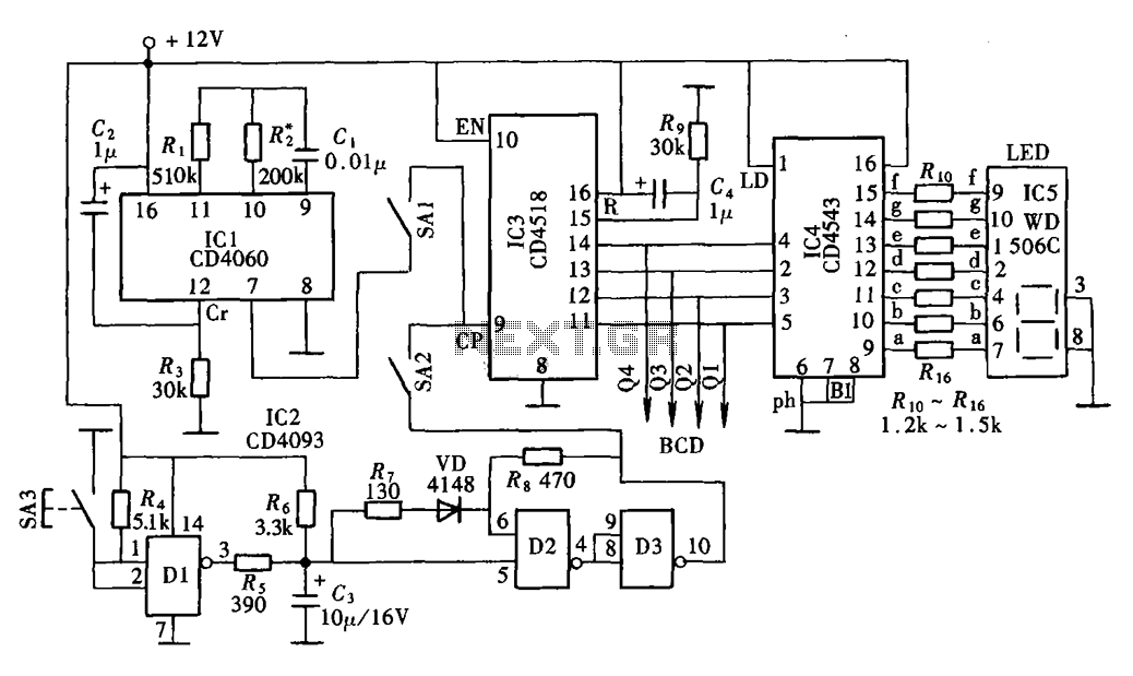
The digital display clock signal source circuit depicted in the figure is derived from a multi-point detection control box within the actual circuit. It primarily comprises an automatic and manual pulse generator, a clock pulse generator, pulse counting elements,...