
Electronic CD4017 CD4066 the switch circuit diagram
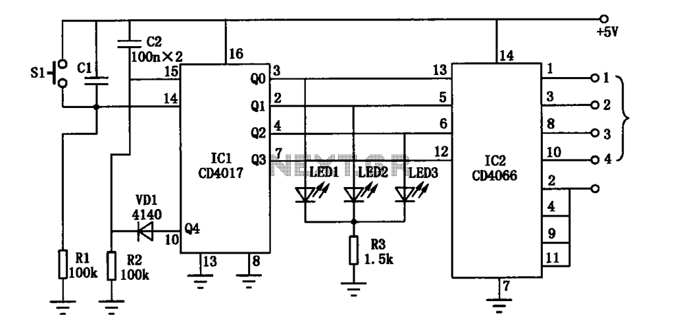
The CD4017 is a decade counter integrated circuit (IC) that can drive up to ten outputs, sequentially activating them based on clock pulses. It is commonly used in applications requiring counting and sequencing. Each output pin (Q0 to Q9) goes high in response to a clock signal, allowing for the control of various devices or circuits.
The CD4066 is a quad bilateral switch IC that can control analog or digital signals. It contains four independent switches that can be used to connect or disconnect signals from a circuit. The switches are controlled by digital signals, allowing for versatile applications in signal routing and manipulation.
In the switch circuit diagram utilizing both the CD4017 and CD4066, the output pins of the CD4017 can be connected to the control inputs of the CD4066 switches. This configuration allows the activation of specific switches based on the counting sequence of the CD4017. For instance, as the CD4017 counts from 0 to 9, it can enable different paths in the circuit, effectively routing signals through the CD4066 switches.
To implement this circuit, the CD4017 would be connected to a clock source, which could be a simple oscillator circuit generating pulses. The outputs of the CD4017 would then connect to the control pins of the CD4066. The input signals to the CD4066 would be routed from the source, and the outputs could lead to various destinations, such as LEDs, motors, or other electronic components.
This configuration allows for dynamic control of multiple outputs using a single clock signal, making it ideal for applications in timing, sequencing, or automated control systems. The combination of the CD4017 and CD4066 provides a flexible and efficient means of managing multiple signal paths in electronic designs.Electronic CD4017, CD4066 constitute the switch circuit diagram:
Related Circuits
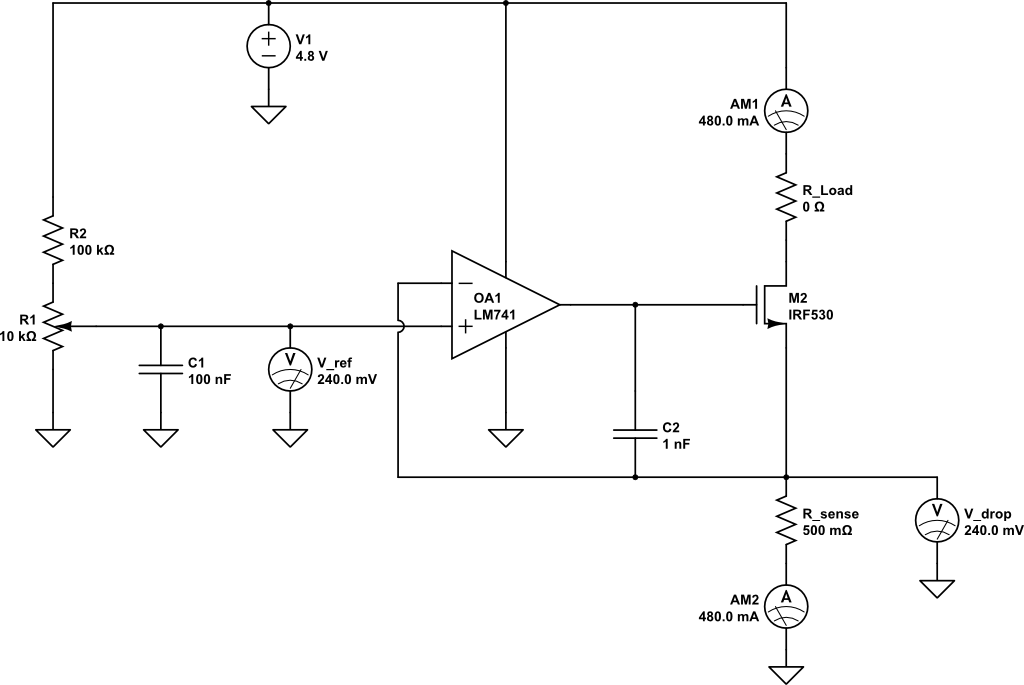
A current limiting circuit is designed to select a maximum current through a load, set to a maximum of 480 mA. As the load resistance increases, the series equivalent resistance (SER) of the limiting circuit decreases. When charging a...
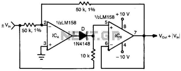
When the input voltage is positive, the output of ICA is negative, resulting in diode D not conducting; therefore, the output of ICB is positive. Conversely, when the input is negative, the output of ICA becomes positive. Diode D...
While many power supplies can be set to limit their output current to a defined level to protect the circuit they are powering, no such protection is available. To enhance the safety and reliability of electronic circuits, it is crucial...
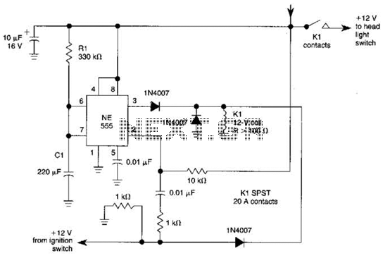
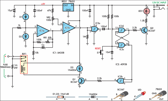
When the ignition switch is activated, relay K1 receives continuous power, allowing the headlights to be turned on. When the ignition is turned off, timer IC1 is activated, maintaining its power for a duration determined by resistor R1 and...
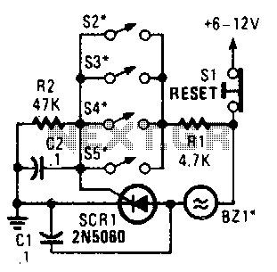
Four parallel switches are employed to monitor four positions. When any switch is closed, SCR1 is triggered, activating the alarm. The alarm is designed to be of the non-interrupting type. The circuit consists of four parallel switches, each representing a...
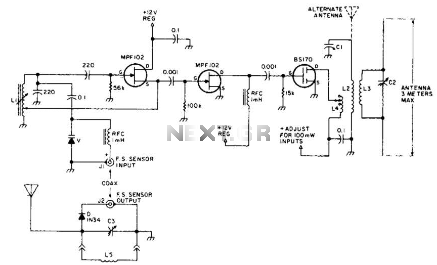
This field strength meter consists of a tuned crystal detector that generates a DC output voltage from a transmitted signal. The DC voltage is utilized to modulate the frequency of a transmitter with a power output of 100 mW,...