
Extensible Multiple Device Programmer 4 Base

The circuit design integrates various components to achieve the intended functionality. The microcontroller serves as the central processing unit, managing communication and control tasks. The RS-232 and RS-422 interfaces facilitate connectivity with external devices, enabling data transfer and device programming. The use of voltage regulators ensures that the microcontroller and associated components receive stable power, crucial for reliable operation. The resettable polyswitch fuse enhances safety by preventing damage from short circuits, while the shorting diode provides an additional layer of protection against incorrect voltage connections. The design's emphasis on using tantalum capacitors reflects a focus on performance, particularly in minimizing power loss and maintaining signal integrity. The dual DAC outputs allow for versatile analog signal generation, catering to various application needs. Overall, the schematic represents a well-thought-out integration of components that supports both functionality and safety in electronic device operation.The 5 volt microcontroller interfaces to the RS-232 serial connector and the USB-B connector. It is also responsible for talking to the checker, controlling the status LED`s and setting the voltage for the LOW voltaage microcontroller. The low voltage microcontroller is run at the voltage level appropriate for programming the device to be programm
ed. It has direct control over a 24V DAC and a 8V DAC. The customization plug is just a large number of female pins for routing power and signals to the 40-pin ZIF socket. One half of the customization plug is hooked to the low voltage microcontroller. The power supply uses a Underwriters Labratory ® approved "wall wart" to provide 24VDC of power. This means that the base board does not have any 110 AC or such voltages running around on it. The power comes in on either N1 (on board) or N3 (off board). The power switch can either be on board at SW1 or off board as SW2 through connector N2. A resettable polyswitch fuse is used to deal with short circuits at F1. D1 is a shorting diode that should trigger F1 if somehow a VAC power source gets plugged into N1 or N3.
The rest of the power supply a series of inexpensive linear voltage regulators, VR1-VR5, that step the voltage from 24 volts, to 18 volts, to 12 volts, to 8 volts and finally to 5 volts. All of these supplies are used elsewhere on the board except the 18 volt one, which is used to keep the 24 volt regulator, VR1, from disapating too much heat.
The capacitors are tantalum for their low series resistance. This design will not win any energy conservation awards, but since the EMPD3 should spend 99% of its time turned off, there should be no real complaints. Finally, green LED D2 lights up to indicate that the device is turned on. The EMDP4 is a board that uses standard serial communcations protocols. Connector N6 is used connect to a DB9 port on a host computer that uses RS-232 voltage levels for signalling.
U7 in conjunction with C7 through C10 converts the RS-232 levels to 5 volt levels. Connector N7 uses a RJ45 jack to provide RS-422 using SimpliciNet pin outs. The nifty DS8921AT at U10 provides RS-422 to 5 volt signalling level conversions. U9A OR`s the recevied signal from U7 or U10 and forwards the signal to the slave microcontroller (U1), the master microcontroller (U2), and to some gating circuitry that potentially gates the signal onto one of the bi-directional bus lines. U9B OR`s the transmit signals from the slave microcontroller (U1), the master microcontroller (U2), and through some gating logic with U8, potentially one of the bi-directional bus; the OR`d signal is forwarded to both the RS-422 connector and RS-232 connector.
U1 is the back processor is a low-voltage PIC16LF877. This microcontroller has direct access to all 30 of the bidirectional lines. The remaining two lines are LVPRX for serial data recieve, LVPTX for serial data transmit. The adaptor boards can be connected to the bus via the 37-pin female D connector N4. Upon startup, the coprocessor is in charge. It immediately asserts LVPRESET# to force the low voltage processor into the reset state. Eventually, it will get around to setting VIO to the correct voltage and will release LVPRESET#. After that, the low voltage processor initializes itself and forces the bus lines to high impedance. Next, the programming algorithm is downloaded over the serial lines LPVRX and LVPTX. Lastly, the STB signal is on RA5 of microcontroller U1. This pin has an open collector output an needs to be pulled high by R21. The data coming back from the IDDAT line is pulled high by R22 to detect when there is now adaptor/plug connected to the system. The digital to analog converter is implemented by U15, a serial quad 8-bit D/A. All of the reference voltages are tied to 2. 5 volts. D/A output A is used to generate VAR1, a 0 to 24 output in. 1 volt increments. D/A output B is used to generate a 0 to 10 volt output in. 🔗 External reference
Related Circuits

The circuit is straightforward. A 555 timer integrated circuit (IC) is utilized to generate a pulse every 20 milliseconds, with a duty cycle ranging from 5% to 10% (1-2 milliseconds). All components used are standard parts. This circuit can...
The audio ground is completely isolated from the digital ground. The top copper layer is utilized as a shield for both the audio and digital ground, which aids in preventing the audio section from picking up noise from the...
In industrial production, flow measurement is a widely used physical quantity measurement. Under specific circumstances, such as when vertical externally positioned installation probes are required for challenging pipelines like oil wells, it is necessary to design instruments and equipment...
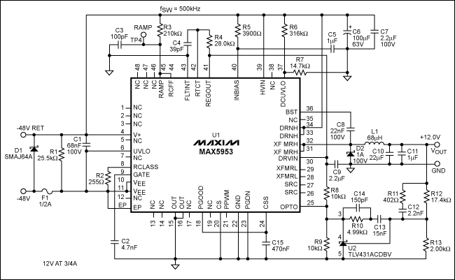
The MAX5953A offers a straightforward, cost-effective, and comprehensive non-isolated power integrated circuit (IC) solution for Powered Devices (PD) in Power-over-Ethernet (PoE) systems. The MAX5953A is designed to facilitate the implementation of Power-over-Ethernet applications by providing an efficient means of...
Planning to base a QRP transmitter on an instructables project, utilizing a large collection of 555 integrated circuits available. The issue is that this transmitter is designed to operate slightly below the commercial AM band. The goal is to...
Various circuit variations have been explored, including a standalone preamp, headphone amplifier, replacements for the 321/729 circuits, and a potential active crossover, depending on demand. There has been significant interest in these designs, and the bootstrap buffer preamp is...