
FET based audio preamplifier
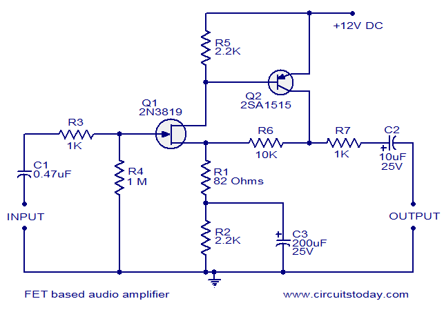
The described audio preamplifier circuit is designed to amplify low-level audio signals with minimal noise interference. The use of a Field Effect Transistor (FET) at the input stage is critical for achieving high input impedance, which allows the circuit to interface effectively with various audio sources without loading them down. The FET Q1 acts as the primary amplifying element, where the audio signal is coupled to its gate via capacitor C1. This capacitor blocks any DC component from the input signal, ensuring that only the AC audio signal is amplified.
Resistor R3 serves as a biasing element, setting the appropriate operating point for FET Q1. The output from the drain of Q1 feeds directly into the base of bipolar junction transistor (BJT) Q2, which further amplifies the signal. The BJT is known for its higher current gain compared to FETs, which is advantageous in this configuration for achieving a significant increase in output signal strength.
The collector of Q2 is where the amplified audio signal is taken as the final output. The presence of capacitor C3 in the feedback loop is essential for stability; it introduces negative feedback that helps to mitigate any potential oscillations that could arise due to the high gain of the circuit. This feedback mechanism also contributes to a more linear response, improving the overall fidelity of the audio output.
Capacitor C2 is positioned at the output stage to decouple any DC component from the amplified signal, allowing only the AC audio signal to pass through. This is crucial for connecting the preamplifier to subsequent audio processing stages, such as power amplifiers or tone control circuits.
The overall design of this preamplifier circuit, with its specified bandwidth of 10 kHz to 450 kHz, makes it suitable for a wide range of audio applications, ensuring that it can faithfully reproduce audio signals across a broad frequency spectrum. The high input impedance of approximately 1 MΩ further enhances its versatility, allowing it to be used with various audio sources without significant signal loss.This is the circuit of a based audio preamplifier which has very low noise. One FET and one BJT are used in this circuit. The audio signal to be amplified is coupled to the base of FET Q1 using capacitor C1 and resistor R3. Base of transistor Q2 is coupled to the drain terminal of FET Q1. Transistor Q2 provides additional current gain. The final si gnal will be available at the collector of Q2. Capacitor C3 provides necessary negative feedback, which improves stability. Capacitor C2 is an output DC decoupling capacitor. Since an FET is used in the input stage this particular amplifier circuit has very high band width (10 KHz- 450 KHz) and input impedance (around 1M). 🔗 External reference
Related Circuits

The ongoing debate regarding the superiority of valves versus transistors is not the focus here. However, for those undecided, this simple amplifier serves as an excellent test. It employs a valve as a pre-amplifier and a MOSFET in the...
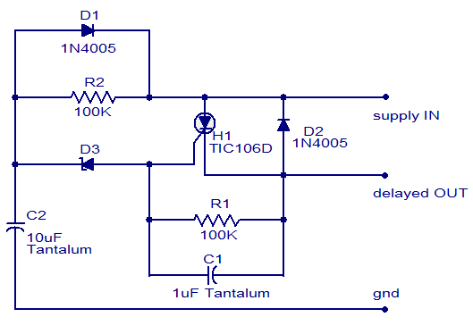
The circuit diagram presented illustrates a straightforward DC power delay circuit that utilizes a Silicon-Controlled Rectifier (SCR). This circuit is highly versatile and applicable in various scenarios. The operation is uncomplicated: when the input power is supplied, capacitor C2...
The input capacitor is used for low-frequency cut-off, with a standard value of 0.1 µF, resulting in a cut-off frequency of approximately 16 Hz. The input capacitor plays a critical role in electronic circuits, particularly in signal processing and audio...
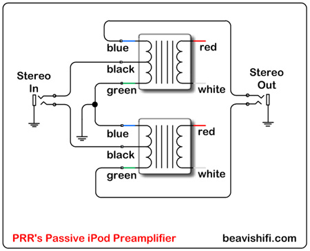
Construct a basic passive preamplifier for use with an iPod, Zune, or other portable media players. This device is particularly useful for enhancing audio quality in a car environment. A passive preamplifier is a circuit designed to amplify audio signals...
The preamplifier is designed for use with dynamic (moving coil, MC) microphones that have an impedance of up to 200 ohms and feature balanced terminals. It is relatively straightforward. The preamplifier circuit serves as a crucial interface between the microphone...
This circuit includes a timed output and an automatic reset feature. It can be manually operated using a key switch or a concealed switch. By incorporating an external relay, the circuit will automatically engage or immobilize the machine each...