
FET high input impedance wideband amplifiers

The described circuit employs a combination of FET and bipolar transistors to achieve a high input impedance preamplifier suitable for wideband applications. The FET operates in a common source configuration, which is known for its voltage amplification capabilities. The Miller effect, which is a phenomenon where the input capacitance appears magnified due to the feedback from the output, poses a challenge at high frequencies. To mitigate this effect, negative feedback is employed, which not only stabilizes the gain but also enhances the bandwidth of the amplifier.
The use of a source follower configuration can further improve input impedance without sacrificing bandwidth. In this setup, the FET is used in a source follower mode to buffer the input signal, providing a high input impedance while allowing for a low output impedance. This configuration is particularly advantageous in applications requiring minimal loading on the preceding stage.
The feedback network consisting of resistors Rs and R3 plays a crucial role in defining the amplifier's overall performance. By adjusting these resistor values, the designer can fine-tune the gain and bandwidth of the amplifier. The feedback loop effectively reduces distortion and enhances linearity, making the amplifier suitable for high-fidelity audio applications or precision measurement systems.
In summary, the integration of FETs and bipolar transistors in a feedback configuration allows for the design of a high input impedance wideband amplifier. This amplifier can be optimized for various applications by adjusting component values, ensuring that it meets specific performance criteria while maintaining stability across a range of operating frequencies.FET has high input impedance, high input impedance amplifier can be made. However, FET amplifying device, the distributed capacitance and the Miller effect input capacitance of the high frequency is very high. In addition, with the rising operating frequency high input impedance FET will also be gradually reduced. Therefore, without negative feedback common source FET amplification is not possible to obtain a very high input impedance over a wide frequency range.
So a high input impedance FET production of wideband amplifier, plus a series of negative voltage feedback amplifiers should be used or the use of source follower plate. Figure 8-11 is a FET, and a bipolar transistor group into a wideband high input impedance preamplifier.
Figure, FET common source amplifier VTi composition, its drain output of the transistor is coupled directly to Cape bamboo base o VT2 VT2 collector output and after Rs and R3 voltage divider is fed back to the flooded VTi pole is formed series voltage deep negative feedback, which greatly improved the frequency response of the amplifier, and increase its input impedance. Figure each component values, the circuit voltage gain Kv 2.7, the output impedance equal to 80n, pass -band of several megohms.
Rs can be improved to increase the overall amplifier gain, Kv may be greater than 100-fold. But with K, mention high frequency response, along with the decrease.
Related Circuits
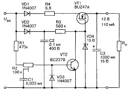
Transformerless power supply FET power supply. Refer to that page for an explanation about the related circuit diagram. It is often required to supply electricity to the consumer at low voltage, specifically 220V. An external adapter can be used,...
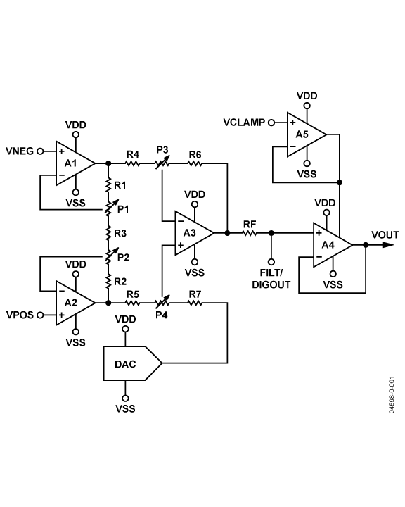
The AD8555 is a zero-drift sensor signal amplifier featuring digitally programmable gain and output offset. It is designed to effectively and accurately convert variable pressure sensor and strain bridge outputs into a well-defined output voltage range. Additionally, the AD8555...
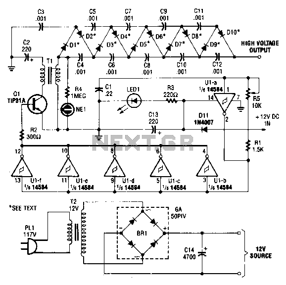
This circuit is powered by a 12-V DC power supply. The input to the circuit is amplified to generate a 10,000-V DC output. The output of the up-converter is subsequently directed into a 10-stage high-voltage multiplier to achieve a...
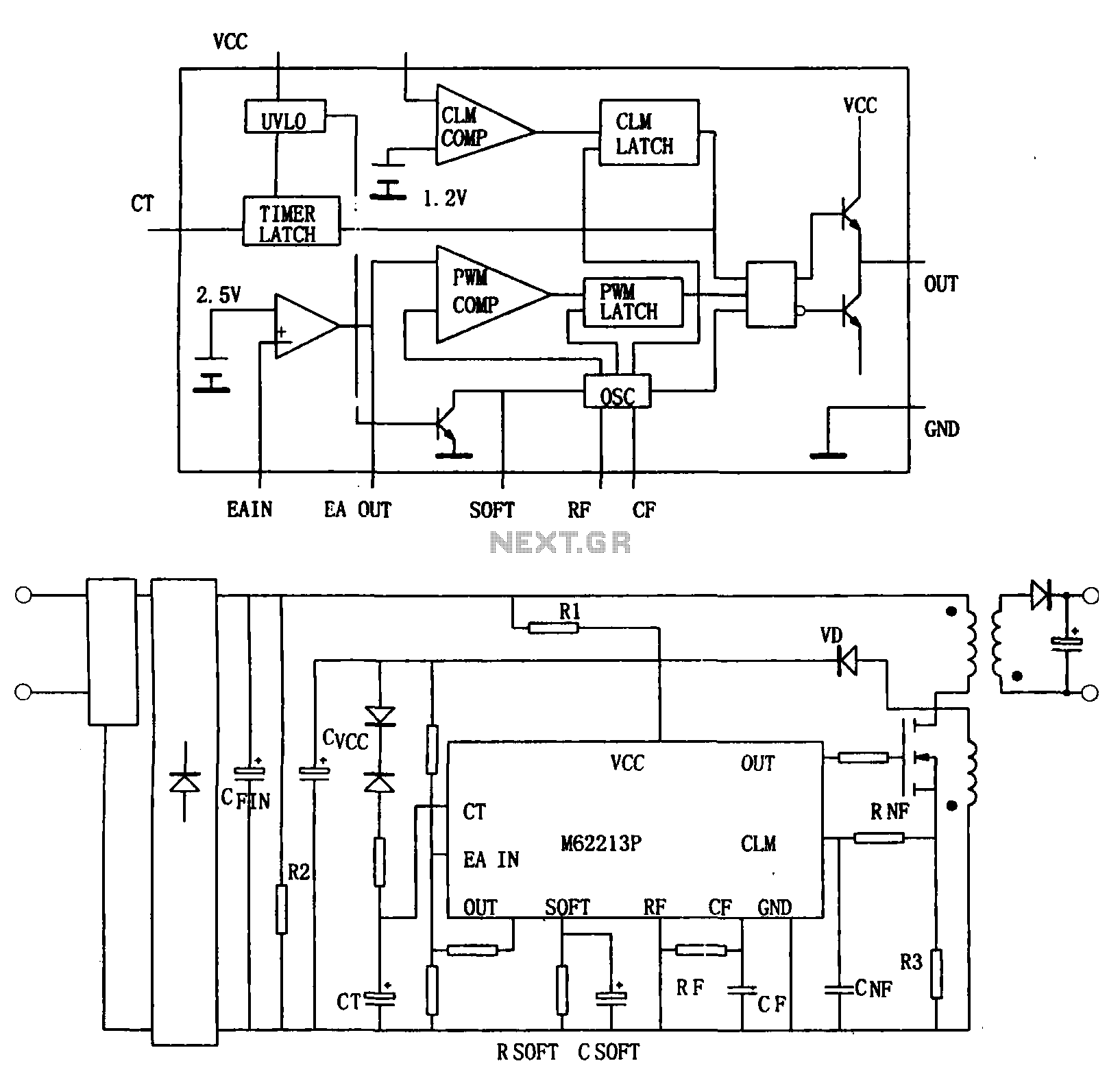
Figure (a) illustrates a block diagram of the internal architecture of the M62213FP, which is a high-speed switching power supply controller. This device includes an oscillator, PWM comparator, error amplifier, output circuit, over-voltage protection, timing latch circuit, over-current protection...
The "R-h sampling circuit limit order" aims to reduce the sampling resistor. A DC voltage level can be positioned between the components. The circuit includes a line amplifier that allows for magnification adjustments and is designed to protect against...
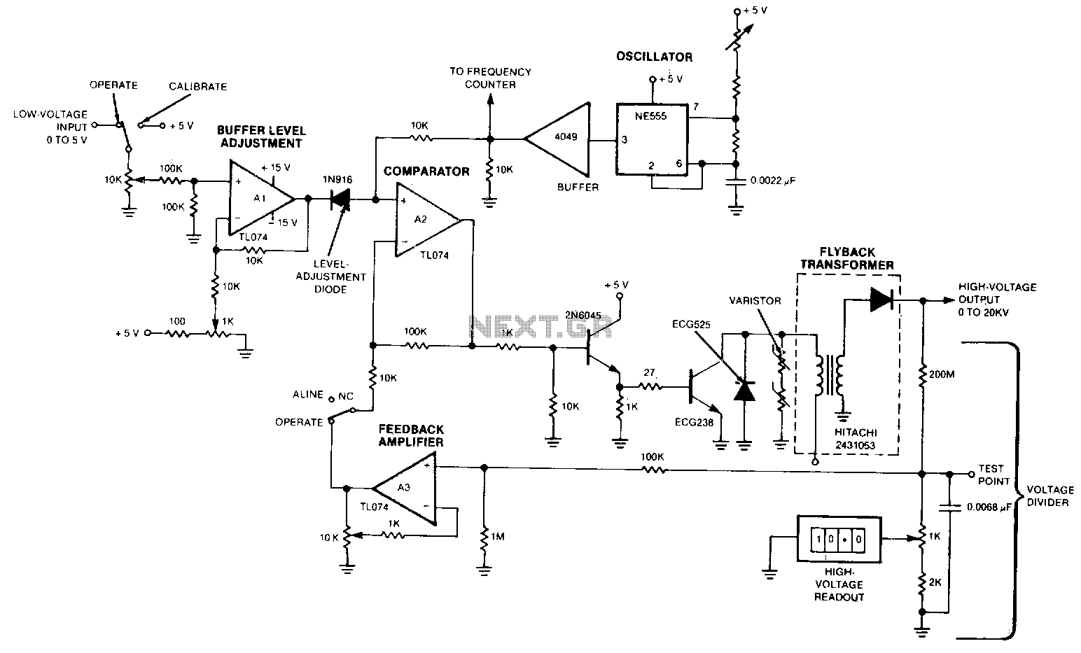
The output voltage varies approximately linearly up to 20 kV as the input voltage is adjusted from 0 to 5 V. A 5-0 potentiometer is used to tune the oscillator, optimizing the output voltage at the frequency of maximum...