
FET Preamplifier
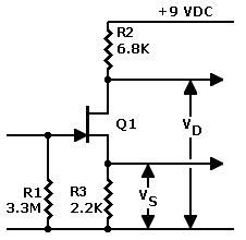
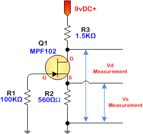
The J201 JFET is a voltage-controlled device that operates effectively within specified parameters. When constructing circuits utilizing the JFET, attention must be paid to the biasing conditions and the selection of resistors. The design should ensure that the drain resistor is larger than the source resistor to achieve the desired gain characteristics. The circuit's performance can be further optimized by careful selection of the source resistor and the use of bypass capacitors to enhance frequency response. The inclusion of a high-value capacitor in parallel with the source resistor allows for improved high-frequency gain while potentially compromising low-frequency performance. Therefore, the choice of capacitor value should be made based on the application's specific frequency response requirements.
In summary, the successful implementation of a JFET-based amplifier circuit hinges on meticulous biasing, component selection, and an understanding of the trade-offs involved in achieving the desired gain across a range of frequencies. Proper adjustments to the source and drain resistors, in conjunction with effective bypassing techniques, are essential for optimizing circuit performance.J201 JFET works best at 10 volts. The minimum current is 0. 5 mA. These are all ideal specifications. The specification spread of FETs is normally three to five times. I`ve personally seen a five-X variation in brand-name devices. The devices that I`ve recently tested are from the same batch. These devices perform more like one another. I intend to operate the test circuits from a 9-volt, regulated power supply. My goal for proper bias of the MPF102 is 4. 5 to 7 volts at the FET drain. If the MPF102 doesn`t bias properly, I`ll perform a second set of tests. In these tests, I`ll take the MPF102 circuit and swap in source resistors. When I find a source resistor that produces drain voltage in the range, I`ll rerun the source and drain voltage tests. Then I`ll check to see if the MPF102 produces voltage gain or attenuates the voltage signal. If the drain resistor is substantially larger than the source resistor, the circuit has voltage gain.
This statement assumes that when using these resistor values, the circuit biases the device correctly. I built the circuit on a plug board. Then I plugged in one test device. I powered the device and measured the drain and source voltages. I then replaced the test device with the next device of the same type, and repeated my tests. As I expected, I had to adjust the bias on the MPF102 transistors. The table below summarizes my results. I tested three of each type of JFET. For each transistor, the table has two columns. In the left column, I give the drain voltage. In the right column, I give the source voltage. Also note that I have a second "MPF102" column on the right. Under this heading are three columns. These three columns detail my adjustment to the MPF102 bias. The leftmost column is the new source bias resistor value. The middle column is the new drain voltage. The right column is the new source voltage. The output (drain) voltages on all three J201 FETs are above 7 volts. I`d expect all three to clip when the gate goes negative. Apparently all three devices have more gain than Tillman`s J201 had. For better performance, a builder should decrease the source resistor. The source voltage will then drop, causing the drain voltage to drop, too. In every test of the MPF102, the Tillman 2. 2K source resistor was too small. This too-small value didn`t produce enough voltage to properly bias the device. The output voltage of all three MPF102 devices dropped to around 2 volts. This voltage will guarantee clipping when the gate goes positive. To correct the clipping problem, I provided a second set of MPF102 tests (right columns). In these tests, I increased the source resistor. I tried several resistors, with 6. 8K producing about the best bias. (In one MPF102 test, VD = 6. 6 volts and VS = 2. 36 volts. ) As the table shows, using an MPF102 in the Tillman circuit causes severe clipping. You can remedy the clipping by increasing the source resistor. Unfortunately, the new source resistor reduces gain to 1 or even attenuates the signal. The upshot: As an amplifier, the circuit fails. There are two ways to correct this problem. Decrease the source and drain resistors, allowing more current to flow through the JFET. Then adjust the source resistor for optimal bias and gain. For gain, the source resistor must be smaller than the drain resistor. Bypass the source resistor with a large-value, electrolytic capacitor. 100 to 1, 000 F should be sufficient. Unfortunately, the gain now varies across the bandwidth. An amplifier with a bypassed source resistor favors higher frequencies. In this circuit, all capacitors are high-pass filters. For better low-frequency response, use a large capacitor value. That`s why I suggest a value as large as 1, 000 F. Effect of Load. The voltage gain formula describes gain into a high-impedance (virtually infinite) load. In the real world, a load of less than some 100K affects the gain. As the load drops belo 🔗 External reference
Related Circuits
JFET iPod preamplifier, DIY Hi-Fi, schematic The JFET iPod preamplifier circuit is designed to amplify the audio signal from an iPod or similar portable audio device, enabling it to drive higher impedance loads such as amplifiers or speakers. This circuit...

A small amplifier with nice characteristics: Tendency of catering: 15V. Force of expense: 4.2Wrms in the 4W. Minimal signal of entry: 94mVp-p with preamplifier, 0.65Vp-p without the preamplifier. More: Materially: R1=2.2kΩ R2=330kΩ R3=4.7kΩ logarithmic potentiometer R4=330Ω R5=1kΩ R6=1.5Ω C1,...
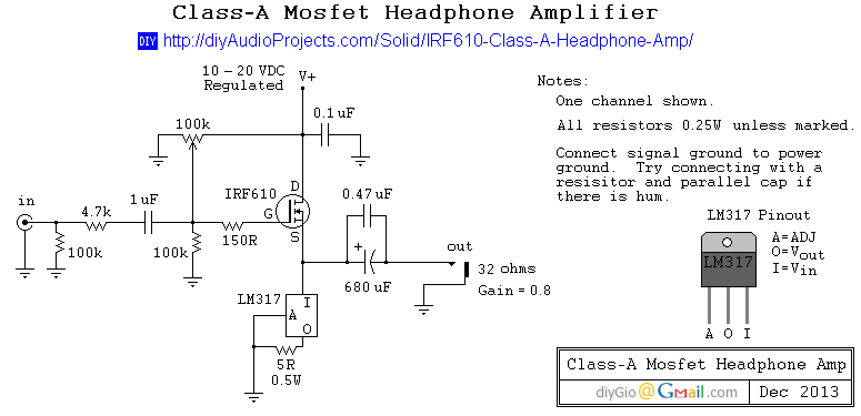
Unsatisfied with the performance of a computer soundcard driving 32-ohm Grado SR80 headphones, a decision was made to construct a desktop headphone amplifier for office use. While ample voltage gain was available, the soundcard struggled with high-quality headphones. This...
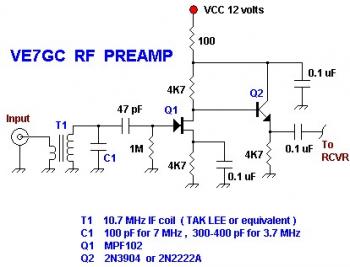
This is a simple VE7GC Popcorn RF preamplifier designed by Dick Pattinson. The circuit features a single tuned circuit at the input stage, allowing direct connection to a mixer or product detector in a straightforward receiver project. Adjustable RF...
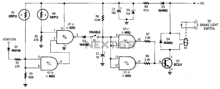
This circuit activates the brake lights of a parked car when headlights from an approaching vehicle are detected, alerting the driver of the oncoming vehicle about the stationary car. LDR4 serves as the sensor, while LDR1 deactivates the circuit...
This simple stereo amplifier utilizes a National LM3871C. The pin numbers in parentheses correspond to one channel, while those without parentheses refer to the other channel. The supply voltage can range from +9 to +30 Vdc at approximately 10...