
Filaments Detection Circuit

The integration of an LCD module with an SST FlashFlex microcontroller involves several key components and considerations. The character LCD typically requires an 8-bit data bus, which facilitates the transfer of data between the microcontroller and the LCD. The control signals are essential for managing the operation of the LCD, with three primary control lines: Register Select (RS), Read/Write (RW), and Enable (E). These signals dictate whether the data being sent is a command or character data, the direction of data flow, and when the LCD should read the data present on the data bus.
In the described implementation, ports P1 and P3 are utilized for direct bit-banging of the data and control signals. This method provides flexibility in programming, allowing the microcontroller to control the timing of the signals manually. The alternative memory-mapped I/O approach, utilizing ports P0 and P2, can simplify the code by allowing the microcontroller to interact with the LCD as if it were a standard memory device, thus leveraging the inherent addressing capabilities of the MCU.
The power supply for the LCD module is critical, as it usually operates at 5V. Additionally, the inclusion of backlight pins can enhance visibility, particularly in low-light environments. The schematic design should ensure proper connections for power, ground, and signal lines, adhering to the pin configuration outlined in the LCD module's datasheet.
When designing the circuit, it is also important to consider the timing requirements specified in the LCD datasheet, particularly for initialization and command execution. Delays may be necessary between commands to ensure that the LCD has adequate time to process instructions. The use of appropriate pull-up or pull-down resistors may also be necessary depending on the specific characteristics of the LCD module and the microcontroller's I/O configuration.
Overall, the schematic design for interfacing an SST FlashFlex microcontroller with a character LCD module should focus on robust signal integrity, adherence to timing requirements, and flexibility in implementation to accommodate various applications in embedded systems.LCD modules have become a popular way to Display system messages and status in embedded applications. This application note shows how to Interface an SST FlashFlex ® microcontroller1 to a typical character LCD module.
The SST FlashFlex is an industry-standard, 8051-compatible MCU and thus gives full control of its I/O ports allow- ing for a variet y of hardware/firmware implementations of the LCD Interface For simplicity, our sample implementa- tion uses ports P1 and P3 of the MCU as bit-banged I/O. However it is also possible to implement the Interface with a memory-mapped I/O scheme, using ports P0 and P2 as a data and address bus.
2. 0 HARDWARE SCHEMATICS The hardware schematic in Figure 2-1 is applicable to most character LCD modules because they conform to the same industry-standard pin assignments and instruction set. The signals to the LCD module consists of an 8-bit data bus, power signals, three control signals, and optionally two pins for a backlight ; This project is LCD Interfaces to standard 8051 MCU such as ; SST89E516RDx, SST89E58RDx.
. 🔗 External reference
Related Circuits
A brief background is provided, indicating a basic understanding of electronics, including knowledge of component functions and schematic reading, but lacking further expertise. The circuit in question appears to involve fundamental electronic components, which may include resistors, capacitors, diodes, transistors,...
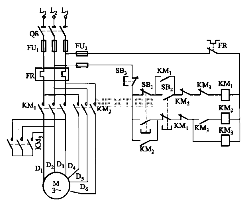
The circuit depicted in Figure 3-96 features a low-speed operation button (SBz), a high-speed operation button (SBi), and a stop button (SB3). In this configuration, a motor is connected in such a way that when the low-speed button is...
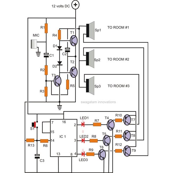
A home intercom system can be constructed using a versatile circuit design. This system allows communication across up to ten different locations or rooms discreetly. It utilizes a single changeover switch for selecting the desired location, replacing the traditional...
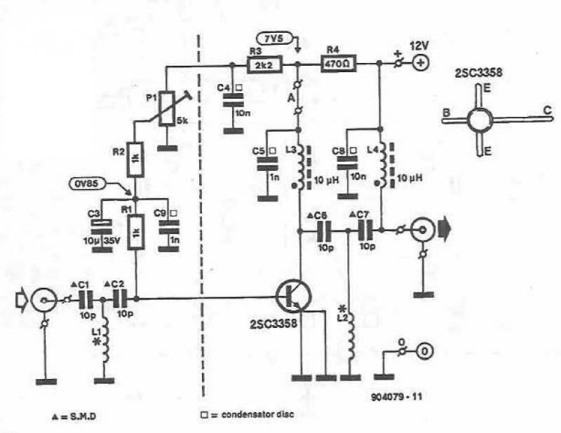
This UHF amplifier circuit project is beneficial for enhancing weak TV signals. The amplifier provides a gain of 10-15 dB within a frequency range of 400 to 850 MHz. To ensure optimal performance and reliability, the PCB tracks should...
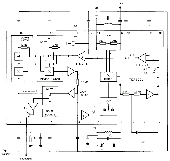
GENERAL DESCRIPTION The TDA7000 is a monolithic integrated circuit designed for mono FM portable radios or receivers, emphasizing minimal peripheral components to achieve compact dimensions and reduced costs. This integrated circuit features a Frequency-Locked-Loop (FLL) system with an intermediate...

This is a white LED lamp that activates when the telephone rings. The cool white light aids in locating the phone in low-light conditions and assists in managing clutter. The circuit for the white LED lamp that illuminates upon a...