
FM demodulator circuit diagram 567
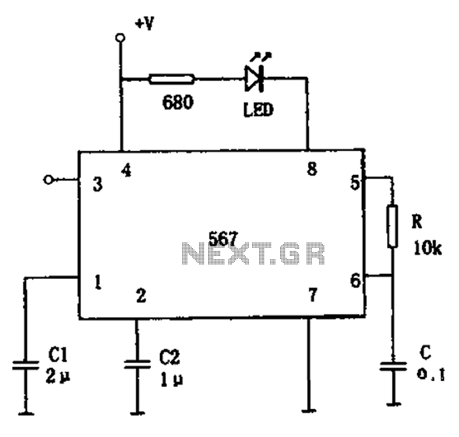
The FM demodulation circuit operates by converting frequency variations in the incoming FM signal into amplitude variations in the output signal. The input signal is fed into the circuit through pin 3, where it is processed to extract the original audio or information signal. The center frequency, fo, plays a crucial role in ensuring accurate demodulation, and it is set according to the formula fo = 1.1/RC, where R is the resistance and C is the capacitance in the circuit.
C1, the filter capacitor, is essential for smoothing out the output signal, minimizing high-frequency noise that could interfere with the clarity of the demodulated audio. C2, the bandwidth adjustment capacitor, allows for fine-tuning of the circuit's response to different frequencies. By adjusting C2, the bandwidth can be increased or decreased, affecting the circuit's sensitivity to adjacent channel interference. A smaller capacitance value for C2 results in a broader bandwidth, which can be beneficial in certain applications where signal strength is variable or where multiple signals are present.
In practical applications, the selection of C2 should be based on the specific requirements of the FM signal being demodulated, including the desired signal-to-noise ratio and the presence of adjacent channel signals. The design of the circuit must also consider the characteristics of the components used, as variations in component values can impact overall performance. The output from pin 5 delivers the demodulated signal, which can then be further processed or amplified for use in audio applications or data transmission systems. Proper layout and shielding of the circuit are also recommended to prevent interference and ensure optimal performance. As shown in Figure 567 FM demodulation circuit. The figure, the FM signal from the input pin 3, the demodulated signal output from 5 feet. FM demodulation circuit can signal ce nter frequency: fo 1.1/RC figure, C1 for the filter capacitor, C2 is the bandwidth adjustment capacitor C2 is reduced when, demodulates the bandwidth increases. C2 is selected on the basis of:
Related Circuits
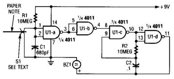
This device prevents paper notes and memos from being overlooked. A paper note placed between two fingers made of a conducting material (metal or conductive plastic) breaks the circuit, allowing pair 1 of Ul-a to go high. The goal...
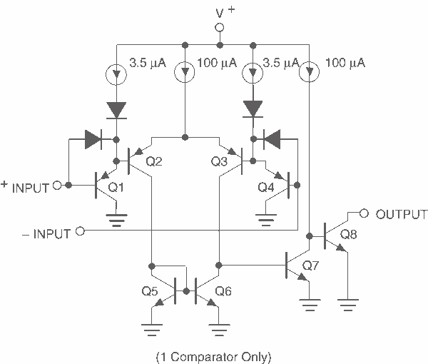
This page provides basic information about voltage comparator integrated circuits and is to act as reference material for other circuits. The circuits shown are based on the LM339 Quad Voltage Comparator chip or the LM393 Dual Voltage Comparator chip....
These small electronic lamps are quite practical and have a long lifespan. Approximately 40 years after Nick Holonyak invented the first LED, they have become nearly essential. Any dedicated electronics enthusiast typically keeps a few in their collection. Prior...
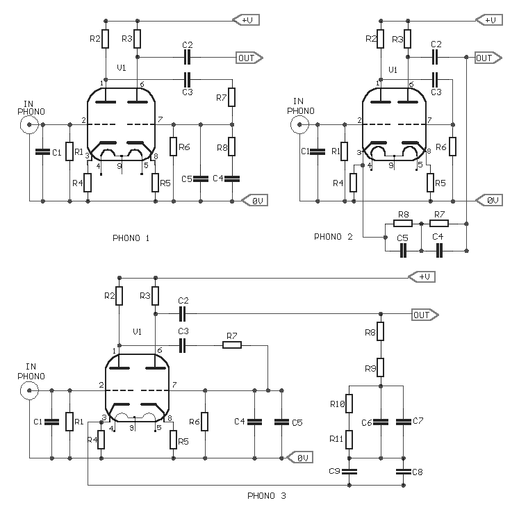
The three circuits were based on the vacuum tube ECC83, designed to produce phono preamplifiers in compliance with RIAA standards. The described circuits utilize the ECC83 vacuum tube, a dual-triode component known for its low noise and high gain characteristics,...
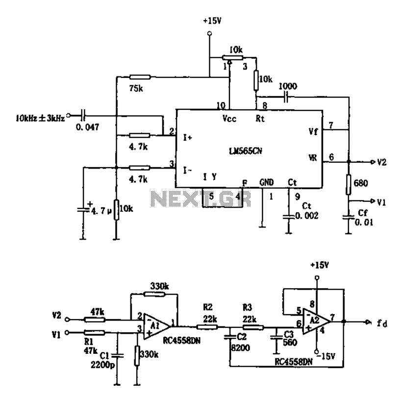
The circuit utilizes a 10 kHz and 3 kHz LM565CN to create an FM demodulation setup. The output diagram (b) illustrates the differential demodulation outputs V1 and V2 from the differential amplifier A1, which provides level displacement and amplification....
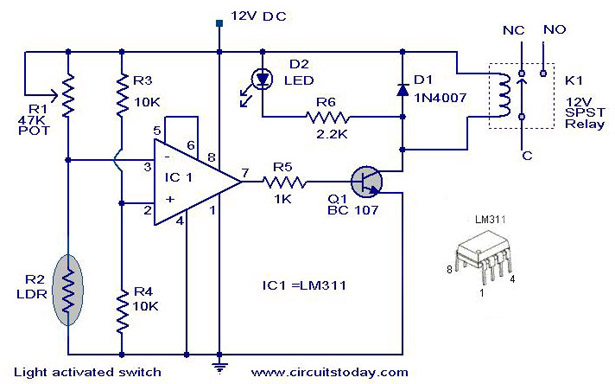
A simple light-activated switch circuit diagram utilizes the National Semiconductor comparator IC LM311 and a light-dependent resistor (LDR). The circuit functions as a voltage comparator, with the non-inverting input of IC1 receiving a reference voltage of 6V through resistors...