
FM modulator strong - weak signal switching circuit
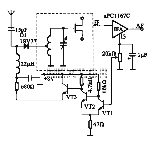
The FM modulator circuit operates by utilizing a switching mechanism that adapts to varying signal strengths. The mechanical switches shown in diagram 3-14 (a) allow for user interaction, enabling the selection of the desired signal strength. This feature is particularly useful in environments where signal quality fluctuates, as it provides the operator with the flexibility to optimize reception.
The diode switching control illustrated in Figure 3-14 (b) plays a crucial role in managing the circuit's response to incoming signals. The diode's ability to switch between conducting and non-conducting states allows for efficient signal processing. When the signal strength is sufficient, the diode is forward biased, allowing the antenna to connect directly to the resonant circuit. This direct connection facilitates a stronger and clearer signal reception.
Conversely, when the signal is weak, the diode enters a reverse bias state, which activates a signal induction process via an inductor into the resonant circuit. This method results in a controlled attenuation of the signal, quantified at approximately 12 to 15 dB. Such attenuation is essential for preventing overload from strong local signals, ensuring that the circuit can effectively discriminate between strong and weak signals.
The intermediate frequency amplifying circuit, as shown in Figure 3-14 (c), is integral to the overall performance of the FM modulator. By amplifying the signal before it is processed through the switching mechanism, the circuit can maintain high fidelity in signal transmission and reception. This design is particularly advantageous in applications where both strong local broadcasts and weaker distant signals must be managed simultaneously, providing a robust solution for diverse signal conditions in FM modulation scenarios.It shows an FM modulator of a strong, weak signal switching circuit. The circuit ring 3-14 (a) shown in mechanical switches, one for the workers selector switch to choose based on the signal strength. Figure 3-14 (b) shows the use of diode switching control. Figure 3-14 (c) shows the use of an intermediate frequency amplifying circuit receives the signal level strength diode control. VT3 control diode bias, when forward biased channel antenna number directly into the resonant circuit, reverse bias to induction via the inductor to the resonant circuit, about 12 ~ 15 dB attenuation of the difference between the two.
This is generally used to attenuate the switching circuit receiving a strong signal (local broadcast) and weak signal (the signal field) antenna input.
Related Circuits
The sensor must be positioned at an angle of approximately 30 to 45 degrees relative to the ground. This orientation facilitates the drainage of rainwater, preventing accumulation that could trigger the alarm due to water retention on the sensor....
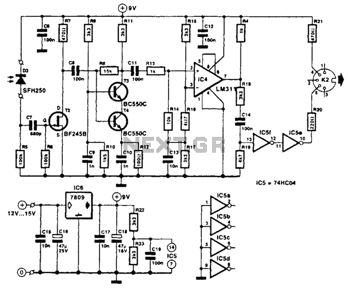
The receiver photodiode SFH250 is utilized to convert optical data pulses at a rate of 32.5 Kbps into electrical signals. The buffer T2 transmits these signals to a cascade amplifier consisting of transistors T3 and T4, followed by an...

The circuit depicted in the figure is designed to achieve a higher power output by modifying specific components. On the left side of the figure, components R1, L1, D1, and capacitors C1 to C7 form a conventional filtering and...
The ADUC812 MicroConverter is a fully integrated 12-bit data acquisition system-on-a-chip. Like all of ADI's MicroConverter products, it features precision A/D and D/A conversion along with a Flash Microcontroller on a single chip. The ADUC812 MicroConverter is designed to provide...
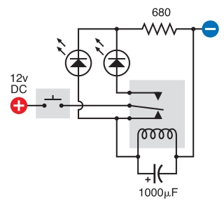
The intended result is for the relay to oscillate and the LEDs to flash when the button is pressed. However, when the button is pressed, the leftmost LED lights constantly, and nothing else happens. There is voltage across the...

The program utilizes the Linear LT1934 chip for the production of a high-efficiency power supply circuit design that is less demanding in terms of electrical load. It offers considerable adjustment margins. When supplied with a 24VDC input, the non-isolated...
Warning: include(partials/cookie-banner.php): Failed to open stream: Permission denied in /var/www/html/nextgr/view-circuit.php on line 713
Warning: include(): Failed opening 'partials/cookie-banner.php' for inclusion (include_path='.:/usr/share/php') in /var/www/html/nextgr/view-circuit.php on line 713