
Low-noise switching power supply schematic circuit diagram
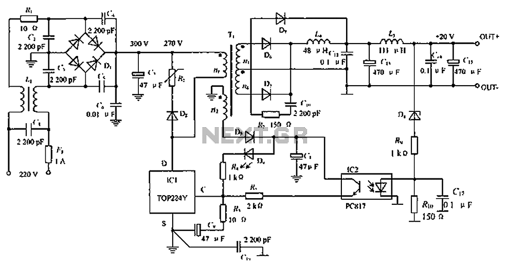
The circuit operates by first converting an AC input into a DC voltage using the rectifying components. The arrangement of R1, L1, D1, and the capacitors (C1 to C7) ensures that the voltage is smoothed and filtered to achieve the desired 30V output. The LC filter on the right, consisting of L5 and C11, further refines the output by attenuating any high-frequency noise that may have been introduced during the conversion process.
The feedback mechanism, facilitated by IC2, D8, R9, and R10, plays a crucial role in maintaining voltage regulation. The feedback loop monitors the output voltage and adjusts the switching elements of the DC-DC converter to ensure that the output remains stable under varying load conditions. This closed-loop control is essential for applications where voltage stability is critical.
In the central section of the circuit, careful attention is given to noise management. This may involve the use of additional filtering components or layout considerations to minimize electromagnetic interference (EMI) and ensure that the circuit operates efficiently. Proper disposal of noise is vital for the reliability of the power supply, particularly in sensitive electronic applications.
Overall, this circuit design emphasizes efficient power conversion, stable output voltage, and effective noise reduction, making it suitable for various applications requiring reliable DC power. Circuit shown in Figure, the circuit can achieve greater power output, just change the part of the device. FIG circuit R1 to the left, L1, D1, C1 to C7 are conventional common mode filtering and rectifying circuit to obtain a DC voltage of about 30V DC-DC converter circuit for use; rightmost circuit L5, C11 and other ordinary LC filter circuit; IC2, D8, R9, R10 voltage feedback circuit composition, form a closed loop structure, stable power supply output voltage; the middle part of the DC-DC converter, the key to reducing noise in this circuit is a part of proper disposal.
Related Circuits
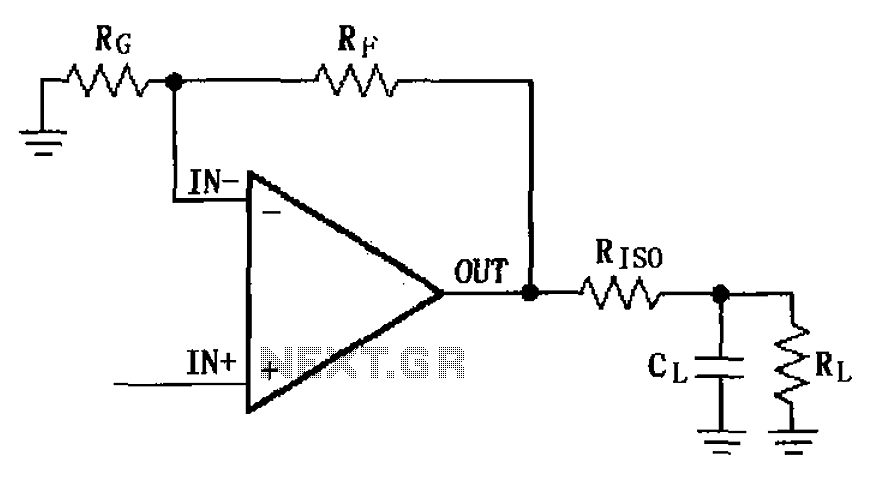
The MAX4223 to MAX4228 series incorporates a capacitive load drive circuit with an isolation resistor (RISO). The maximum allowable capacitive load for these devices is 25pF. However, exceeding this limit can lead to overshoot and ringing. The circuit design...
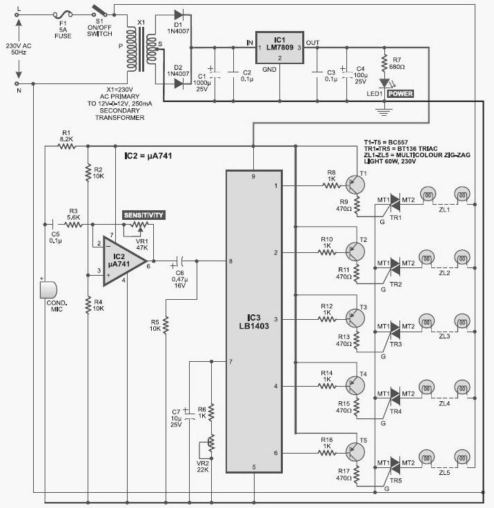
This light chaser circuit, which functions as a music-operated lighting effect generator, consists of five sets of 60W bulbs arranged in a zig-zag configuration. The light chaser circuit is designed to create dynamic lighting effects that synchronize with music, enhancing...
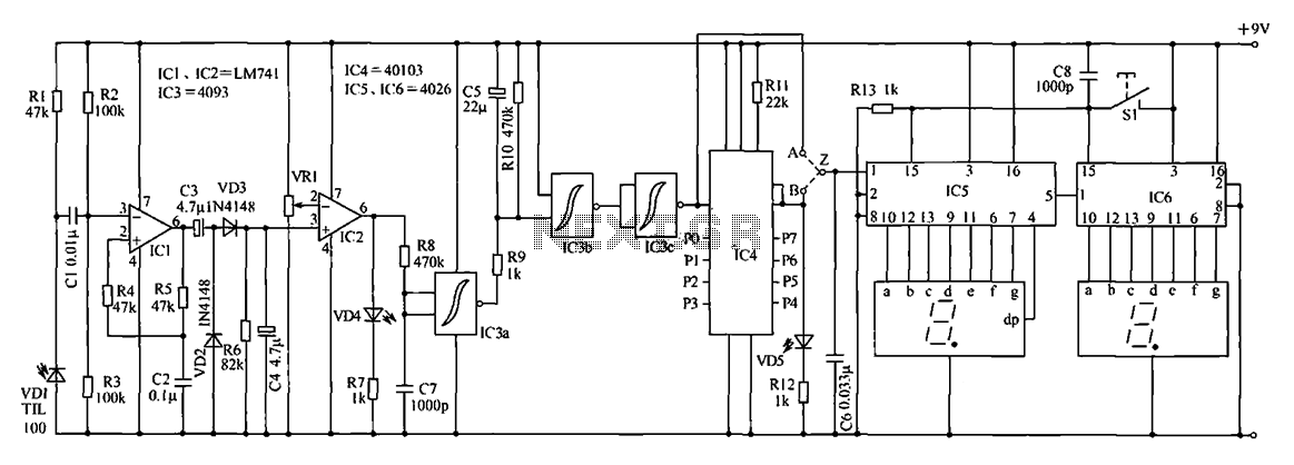
The digital counter circuit described utilizes an infrared signal to detect moving targets, making it suitable for counting small devices on a production line as they move along a conveyor belt. This circuit can also be employed for various...

This software was developed specifically for the hardware in question. Consequently, the pin allocation of the Atmel ATtiny2313 in this circuit corresponds to the original design, allowing the software to operate on both hardware platforms. An important note is...
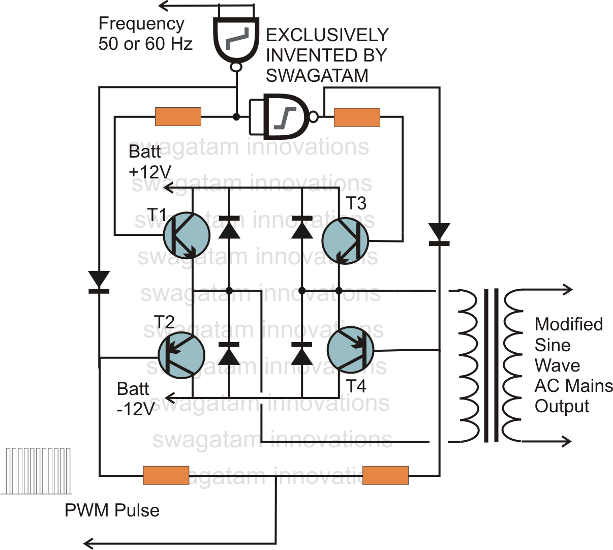
In electronics, an H-bridge circuit refers to a configuration consisting of four individual switching devices, such as transistors or MOSFETs, which can be controlled by external discrete signals from the respective stages of the control circuit. During operation, the...
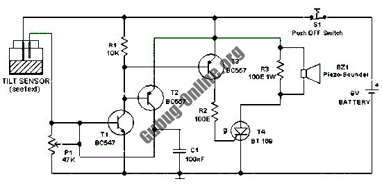
This design features a simple circuit for a tilt sensor alarm that can be constructed using readily available and inexpensive components. The circuit is based entirely on transistor technology. The homemade tilt sensor for this circuit utilizes a standard...
Warning: include(partials/cookie-banner.php): Failed to open stream: Permission denied in /var/www/html/nextgr/view-circuit.php on line 713
Warning: include(): Failed opening 'partials/cookie-banner.php' for inclusion (include_path='.:/usr/share/php') in /var/www/html/nextgr/view-circuit.php on line 713