
fm oscillator with bly87
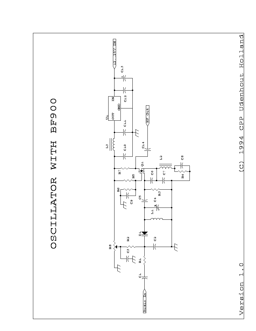
The circuit design primarily features various capacitors and inductors that are essential for the operation of the FM oscillator. The selection of capacitors, including both ceramic and electrolytic types, ensures stability and performance across the desired frequency range. The use of a trimmer capacitor (C4) allows for fine-tuning of the oscillator frequency, which is critical in applications requiring precision.
Inductors L1, L2, and L3 are integral to the circuit, with L1 serving as a tuned circuit element that works in conjunction with the capacitors to establish the oscillator's frequency. The specified dimensions and materials for L1, particularly the use of copper-silver wire, suggest a focus on minimizing resistive losses and enhancing the quality factor (Q) of the inductor. The mounting height of L1 above the PCB is also significant, as it influences the magnetic coupling and overall inductance.
The BF900 dual gate MOSFET is chosen for its low noise characteristics, making it suitable for RF applications. Its design allows for high-frequency operation, which is essential for FM transmission. The recommendation for proper buffering indicates a consideration for signal integrity and the prevention of oscillation instability, which can occur in high-frequency circuits.
Overall, the schematic and layout provided in this package are tailored for efficiency and reliability in FM oscillator design, making it suitable for various applications in communication systems where low noise and stability are paramount.C1=100nF Multilayer or ceramic C2 : 4. 7 pF ceramic C3 : 100 nF ceramic (1 or 10 nF will do also) C4 : 40 pf trimmer C5 : 4. 7 pF ceramic C6 : 10 pF ceramic C7 : 22 pF ceramic C8 : 1 nF ceramic C9 : 1 nF ceramic C10: 100 nF ceramic C11: 100 nF ceramic C12: 100 nF ceramic C13: 47 uF/25V C14: 1 nF ceramic L1 : 4 wdg, dia 8 mm, 1 mm CuAg, space 1 mm ; Mounted 8 mm above PCB (Leads are 4 mm) L2 : 6-hole ferroxcube wideband HF-choke (5 wdg) L3 : 6-hole ferroxcube wideband HF-choke (5 wdg) This package contains the schematic and PCB layout for the FM oscillator using the BF900 Dual Gate MOSFET, which is used between 90 and 110 MHz. and that he has a very low noise, and very stable. If you use the proper buffering, a PLL is not needed anymore. For BF900 mounting holes (diameter 6 mm) should be created in which the casing can survive in. I myself have a problem with the other side of the copper`, since the oscillator will not light (not really enough votes Just kidding).
Was solved when I removed the copper BF900 (about 1 1. 5 cm diameter). 🔗 External reference
Related Circuits
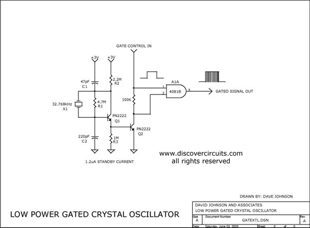
The circuit controls the output of a continuously operating 32KHz crystal oscillator, directing it to the input of a C-MOS buffer when clock pulses are required. This technique addresses the issue of a slow-starting crystal oscillator by maintaining the...
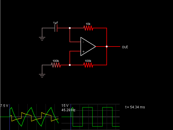
This circuit is an oscillator that generates a square wave. The operational amplifier (op-amp) begins with its two inputs in an undefined state, starting with the non-inverting input slightly higher than the inverting input. The op-amp significantly amplifies this...
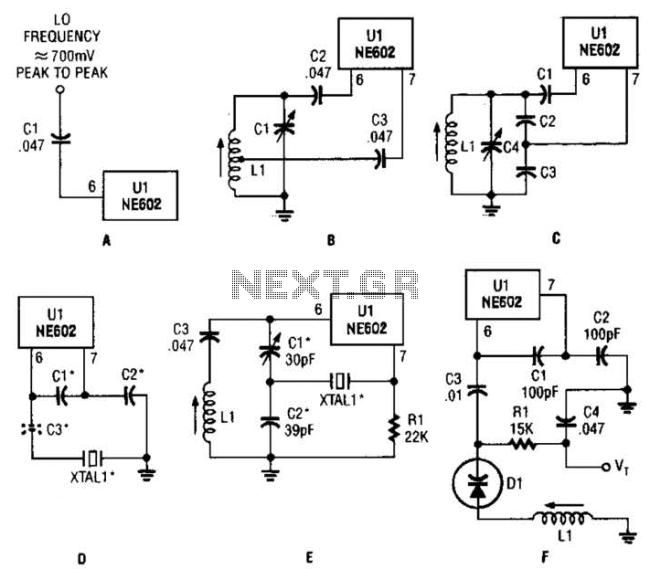
Any standard oscillator, such as a Colpitts or Hartley configuration, can be utilized to generate the local oscillator (LO) frequency required by the NE602. The NE602 is a versatile integrated circuit commonly used in radio frequency applications, particularly in mixer...
A capacitor in series with the crystal may be utilized to adjust the oscillator output frequency. The value may range between 20 pF and 0.01 µF, or it may be a trimmer capacitor, and it will approximately equal the...
This oscillator is a variation of the oscillator presented by Ulrich L. Rohde, DJ2LR, in his article "Evaluating Noise Sideband Performance in Oscillators," published in Ham Radio, October 1978, Page 51. The original circuit can be found at the...
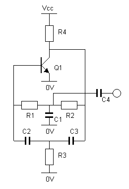
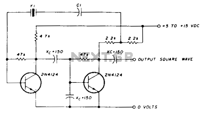
The output of this circuit should be connected to a high-impedance load, typically greater than 100K ohms, while noting that the impedance of capacitor C4 is approximately 3K ohms. A PNP transistor may also be utilized, requiring adjustments to...