
FM Transmitter Circuit Providing 500mW Output

This circuit functions as a frequency modulation (FM) transmitter, capable of delivering an output power of 500 mW. The core of the design consists of four transistors that play a pivotal role in modulating the signal. Each transistor is configured to amplify the modulated signal, ensuring that the transmitter can effectively broadcast over a specified range.
The first stage typically involves a signal generation circuit, which could include an oscillator to produce a carrier frequency. This frequency is then modulated by the input audio signal. The modulation process alters the frequency of the carrier wave in accordance with the amplitude of the audio signal, effectively encoding the information onto the carrier.
The four transistors are arranged in a configuration that may include a combination of common emitter and common collector stages. This arrangement allows for both amplification and impedance matching, which are crucial for maximizing the power output and ensuring efficient transmission. The output stage may also include a matching network to optimize the power transfer to the antenna.
Power supply considerations are critical; the circuit requires a stable DC voltage source to ensure consistent operation of the transistors. Bypass capacitors may be employed to filter out noise from the power supply, thereby improving the overall performance of the transmitter.
In terms of performance, the circuit should be capable of maintaining linearity in modulation to prevent distortion of the transmitted signal. Proper heat dissipation measures, such as heat sinks for the transistors, may also be necessary to ensure reliability during prolonged operation.
Overall, this FM transmitter circuit is designed to operate efficiently within its specified parameters, providing a robust solution for wireless audio transmission applications.The circuit was designed to produce a 500mW output power transmitter whose signal modulated by FM using four transistors. Transmitter an electronic devi.. 🔗 External reference
Related Circuits
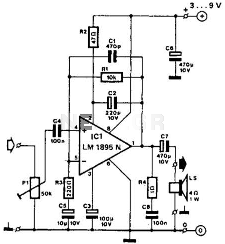
This amplifier operates with supply voltages ranging from 3 V to 9 V and can deliver an output power ranging from 100 mW to 1 W into a 4-ohm load. The bandwidth is approximately 20 kHz at a 3...

The system consists of a MAX1463 precision pressure detection circuit block diagram. The output voltage from the bridge pressure sensor is connected to the MAX1463 inputs IN1+ and IN1-. Controlled by a CPU, the pressure signal undergoes nonlinear calibration...
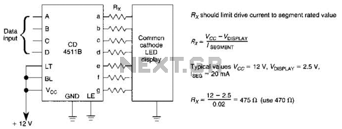
A CD4511B CMOS LED display driver can be utilized to operate a common cathode LED display. Current limiting resistors are employed to restrict the segment current to the specified value at the maximum supply voltage. The CD4511B is a...
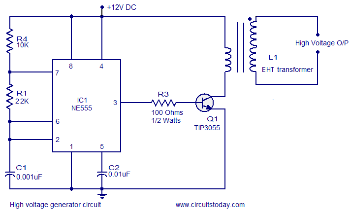
This circuit is highly dangerous due to its output voltage, which is in kilovolts and poses a significant risk of serious injury or death. It should only be attempted by individuals with extensive experience in handling high voltages. No...
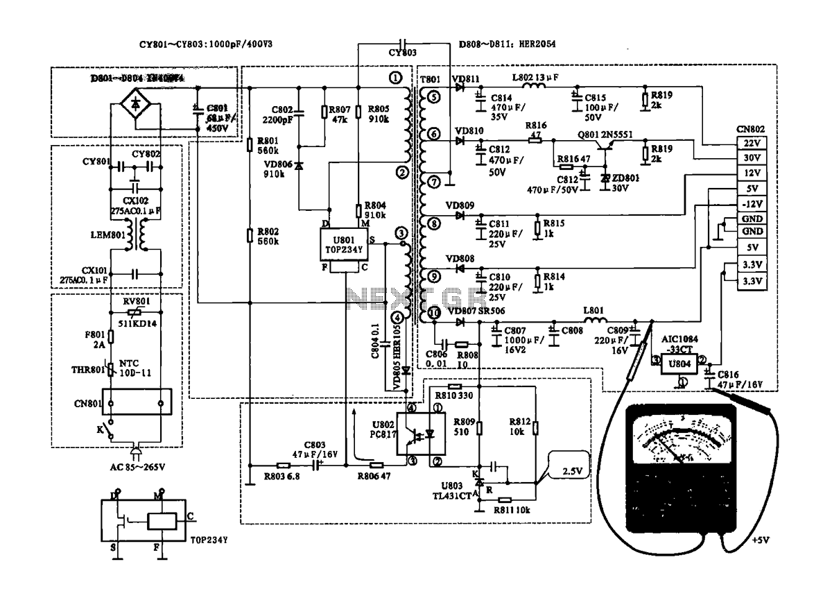
The Coship CDVB3188V receiver features a switching power supply circuit similar to the CDVB3188C model. The circuit includes several key components: an AC input circuit, an anti-jamming filter circuit, a complete flow filter circuit, and a switching oscillation circuit....
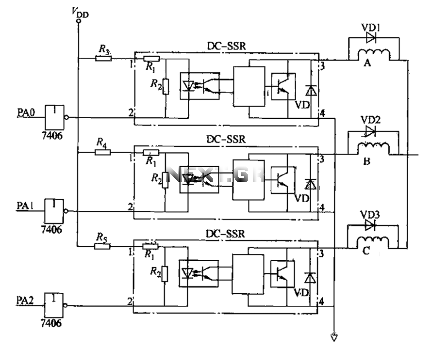
The figure illustrates that the DC Solid State Relay (SSR) in the input stage functions as an opto-isolator. When the switch output is high, the driver circuit inverts this signal to low. This process involves a light-emitting diode (LED)...