
Coship CDVB3188V receiver switching power supply circuit
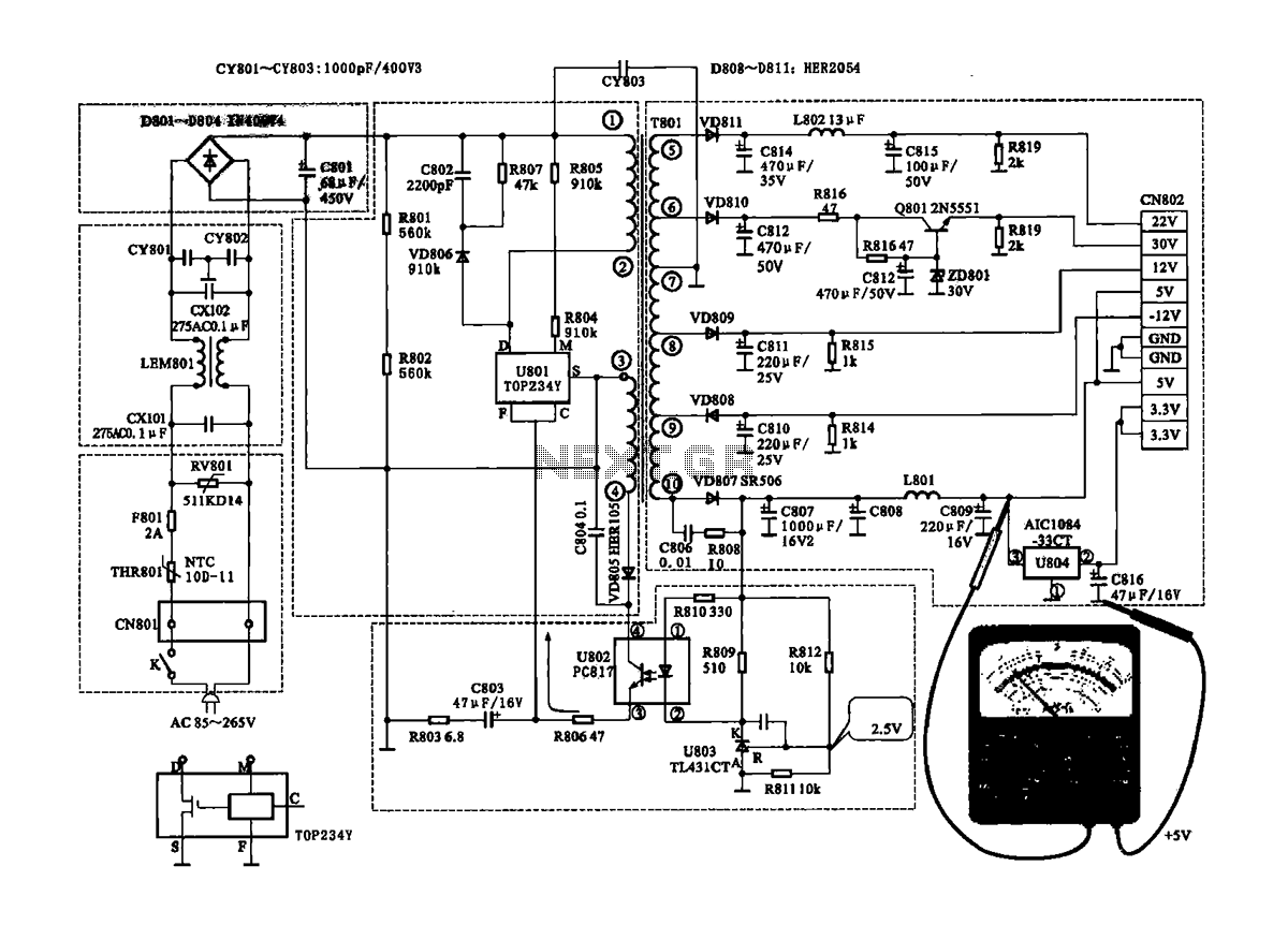
The Coship CDVB3188V receiver's switching power supply circuit is designed to efficiently convert and regulate power for the device's operational needs. The AC input circuit serves as the initial stage, where the power is connected and safeguarded against overvoltage and overload conditions. The inclusion of a thermistor and pressure-sensitive resistors enhances protection, ensuring the device operates safely under varying conditions.
The interference filter circuit plays a crucial role in maintaining the integrity of the power supply by filtering out high-frequency noise that could disrupt the operation of the receiver. This is particularly important in environments with significant electrical interference, as it ensures reliable operation and minimizes the risk of malfunction.
The rectifier filter circuit efficiently converts the incoming AC voltage to a usable DC form. The bridge rectifier configuration enables full-wave rectification, which is essential for providing a steady DC voltage. The smoothing capacitor helps to reduce voltage ripple, ensuring a stable output that is vital for the proper functioning of the subsequent circuits.
The switching oscillation circuit is the heart of the power supply, responsible for generating the necessary output voltages. The use of an integrated circuit allows for precise control of the oscillation frequency and pulse width, which directly influences the output voltage levels. The feedback mechanism involving the photoelectric coupling device ensures that any fluctuations in output voltage are quickly corrected, maintaining a stable power supply for the receiver.
Overall, the design of the switching power supply circuit in the Coship CDVB3188V receiver exemplifies a well-thought-out approach to power management, integrating multiple protective and filtering components to ensure reliable operation and adaptability to varying input conditions.Coship CDVB3188V receiver switching power supply circuit It shows the same continent CDVB3188C receiver switching power supply circuit, mainly from the AC input circuit, anti-j amming filter circuit, the entire flow filter circuit, switching oscillation circuit. (1) AC input circuit is K AC input circuit from the power switch, AC input connector CN801, thermistor THR801, fuses F801 and a pressure-sensitive electrical resistance and other parts of the RV801. As has been the receiver overload fault, the fuse is blown, its protective effect. If the external input voltage is too high (high to 260 V) varistors short circuit, and the fuse is blown, the same protective effects.
(2) interference filter circuit interference filter circuit mainly by the clamor CXI filter capacitor pair, CXl: 02, CY801, CY802 and mutual LEM801 filter element and other components constituted, it is mainly to filter out interference pulses from the alternating current in Argentina, and can also prevent the switching power supply to the anti-oscillation pulse generated electricity to Argentina and cause interference to other equipment. (3) rectifier circuit rectifier filter circuit is composed of a bridge rectifier D801-D804 and the capacitor C801 constitute a filter, and its function is to 220V AC voltage is rectified into direct current (approximately 300V) voltage, and then later by the smoothing capacitor C801 eliminate ripple component, the oscillation of the switching power supply circuit.
(4) switch oscillation circuit switching oscillation circuit mainly by the oscillation switch integrated circuit U801, switching transformer T80], the secondary output voltage regulator circuit and configured into. After the voltage of 30V DC power to the switch as the T801 transformer primary winding O feet, after primary winding feet to the switch by the oscillation of D IC U801 pin, the pin is connected U801 within the drain D of the field effect transistor switch At the same time + 300V DC via the startup resistor is R805, R804 to switch integrated circuit U801 oscillation start voltage of M plus side, the oscillation start oscillation circuit within the U801, U801 then switching field effect transistor within the oscillation signal by the driver go into oscillation.
Switch transformer secondary winding ( ~ end), Kai vibration when feet rectified and filtered to form output voltage and optically coupling device U802 U801 feedback to the F, C terminal. After the start vibrating after switching power supply switching transformer secondary output rectifier filter through the windings of the multiple output DC voltage of the receiver power supply.
Regulator circuit connected to the output circuit of + 5V, + 5V output voltage through R812, R811 constitute a voltage divider circuit, normal voltage dividing point is 2.5 V, the error voltage as the sampling point to the input of the error amplifier U803 R, If the +V output voltage fluctuations cause the sampling point voltage changes, the error voltage is applied to the R terminal U803, U803 KA will cause changes in impedance between the inter-U803 AK impedance variations of the cause of the photoelectric coupling unit U803 changes in the emission intensity of the light emitting diode, thus causing photoelectric coupling vessel phototransistor impedance U802 change the voltage U802 foot wells changed, the voltage signal is applied as a negative feedback oscillation F terminal of the switch IC, so U801 in the oscillation pulse width changes, so that the output switching power supply is stabilized.
Related Circuits
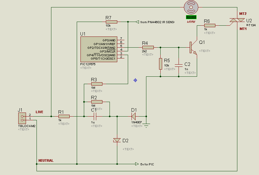
A project is underway to control the speed of an electric fan (220Vac, 60W, 5A max.) automatically using a microcontroller based on certain parameters. The circuit design for controlling the speed of an electric fan involves several key components to...
This document discusses the advantages and disadvantages of various power supply technologies, along with the design considerations necessary for selecting and evaluating a mains transformer. It covers the pros and cons of external supplies, inrush current control, RF emissions...

This is a design circuit diagram of a versatile FM transmitter. This circuit does not include a coil and is simple and easy to assemble. It operates based on gate logic concepts. The circuit features a buffer gate N1...
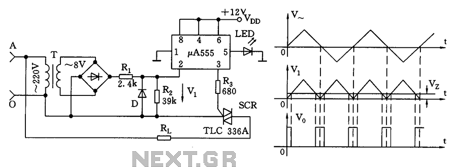
The zero volt switching circuit generates a trigger pulse at the zero crossing of the AC voltage. To facilitate this, the zero crossing of the 555 limit comparator is connected to a single form, with the comparison voltage set...
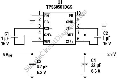
This is a circuit of a step-down charge pump regulator for USB-powered devices. The critical design parameter of this circuit is the circuit area. The step-down charge pump regulator is designed to efficiently convert a higher input voltage from...
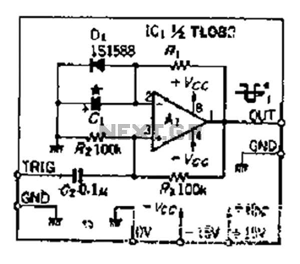
Although people believe that using a timer with an operational amplifier (op-amp) does not yield significant results, it can still be advantageous in certain scenarios. In environments with high noise levels, the application retains its benefits. When the phase...
Warning: include(partials/cookie-banner.php): Failed to open stream: Permission denied in /var/www/html/nextgr/view-circuit.php on line 713
Warning: include(): Failed opening 'partials/cookie-banner.php' for inclusion (include_path='.:/usr/share/php') in /var/www/html/nextgr/view-circuit.php on line 713