
Frequency-to-voltage converter

In this circuit design, the pulse input is processed through a differentiating C-R network, which serves to convert the input pulse into a sharp negative-going edge. This edge is crucial for triggering the comparator connected to pin 6, which subsequently activates the timer circuit. The design utilizes a voltage-to-frequency conversion principle, where the average current (I_average) flowing from pin 1 is calculated based on the equation I_average = i (1.1 RjC^ f). This indicates a direct relationship between the input current, resistance, capacitance, and frequency of operation.
The filtering component of the circuit consists of a resistor (RL) with a resistance of 100 kΩ and a capacitor (C) of 1 µF. This RC filter is designed to smooth out the output current, ensuring that any high-frequency noise is attenuated. As a result, the ripple voltage at the output is maintained below 10 mV peak, which is critical for applications requiring precision and stability in the output signal.
However, the circuit exhibits a slow response time, characterized by a time constant of 0.1 seconds. This indicates that the circuit will take this duration to respond to changes in the input signal. Furthermore, the settling time of 0.7 seconds to reach within 0.1% of the final value suggests that while the circuit is stable, it may not be suitable for applications requiring rapid response times. Overall, this design balances filtering and stability, making it appropriate for specific applications where precision is paramount, but speed is not the primary concern.In these applications, a pulse input at % is differentiated by a C-R network and the negative-going edge at pin 6 causes the input comparator to trigger the timer circuit. Just as with a V-to-F converter, the average current flowing out of pin 1 is IaverAGE = i (1.1 RjC^ f.
In this simple circuit, this current is filtered in the network RL = 100 k ohm and 1 µF. The ripple will be less than 10 mV peak, but the response will be slow, with a 0.1 second time constant, and settling of 0.7 second to 0.1%
Related Circuits
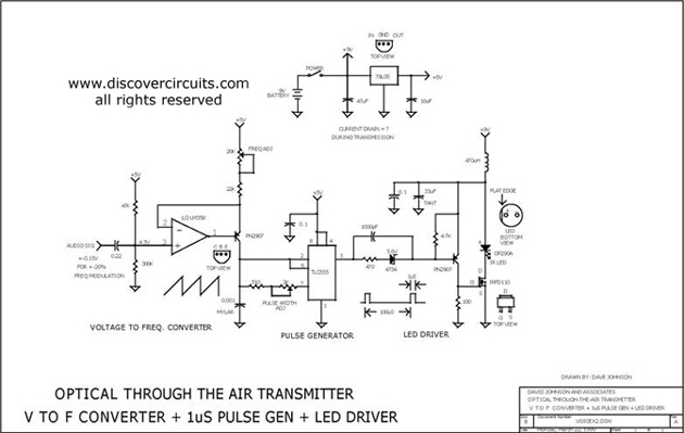
This circuit receives the signal from the amplifier and emits powerful 1μs infrared light pulses from a low-cost LED, which are frequency modulated by the audio information. The 10kHz center frequency of the pulse stream is sufficiently low, allowing...
Simple function generators typically produce sinusoidal, rectangular, and triangular waveforms, but rarely generate sawtooth waveforms. The circuit depicted in Fig. 21-4(a) generates a sawtooth signal from rectangular and triangular signals. The quality of the sawtooth output is influenced by...
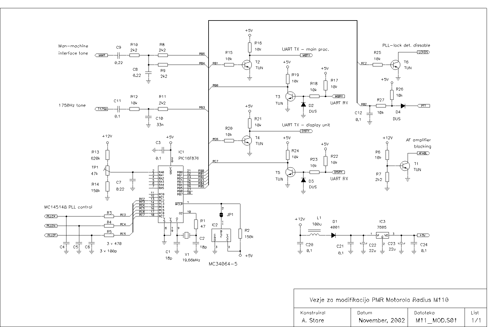
The PMR VHF transceiver Motorola Radius M110 (in further text referred as M110) was manufactured by Motorola GmbH therefore being an European radio. Since many professional radio service users has replaced this transceiver with newer gear, a considerable number...
An Analog-to-Digital Converter (ADC) is a circuit integrated into a single chip designed to convert analog signals into digital signals. Typically, an 8-bit ADC chip converts an analog signal ranging from 0 to 5 volts into a digital level...
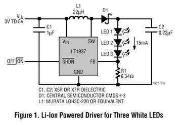
The LT1937 is a step-up DC/DC converter specifically designed to drive white LEDs with a constant current. The device can drive two, three or four LEDs in series from a Li-Ion cell. Series connection of the LEDs provides identical...
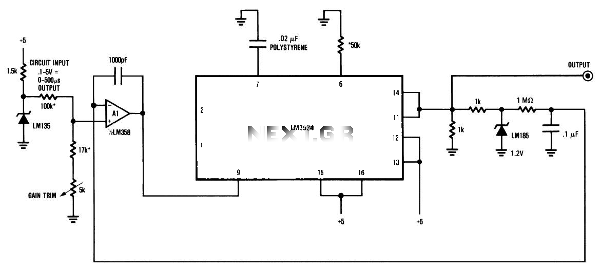
The circuit is a temperature-to-pulse-width converter. The LM3524 is used to convert the output of an LM135 temperature transducer into a pulse width that can be measured by a digital system, such as a microprocessor-controlled data acquisition system. In...