
full-wave rectifier
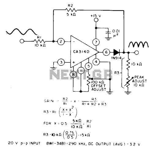
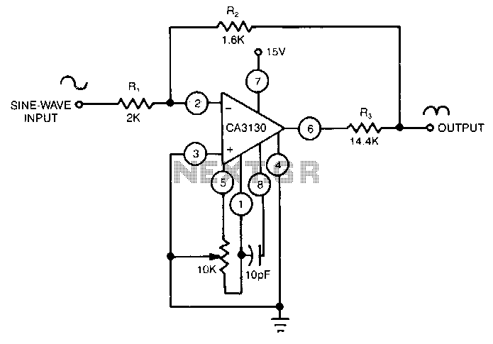
The circuit design featuring the CA3140 BiMOS operational amplifier is characterized by its inverting gain configuration, which is essential for applications requiring signal inversion along with amplification. The CA3140 is notable for its high input impedance and low output impedance, making it suitable for interfacing with a variety of signal sources while minimizing loading effects.
In the inverting configuration, the input signal is fed into the inverting terminal of the op-amp through a resistor, typically denoted as R1. A feedback resistor, Rf, is connected from the output back to the inverting terminal. The gain of the circuit is determined by the ratio of these resistors, calculated using the formula: Gain = -Rf/R1. The negative sign indicates that the output signal is inverted relative to the input.
The symmetrical full-wave output is achieved when the circuit is designed to accommodate both positive and negative input signals, allowing for a complete waveform representation. This is particularly useful in applications such as audio processing and signal conditioning, where maintaining the integrity of the waveform is crucial.
The non-inverting terminal of the CA3140 is typically connected to ground or a reference voltage, ensuring that the op-amp operates within its linear range. Proper power supply decoupling is also critical to prevent oscillations and ensure stable operation, often achieved by placing bypass capacitors close to the power supply pins of the op-amp.
Overall, the implementation of the CA3140 in an inverting gain configuration not only provides the necessary signal inversion but also enhances the performance of the circuit through its high-speed capabilities and low noise characteristics, making it an excellent choice for various electronic applications. When equality of two equations shown in satisfied, full-wave output of circuit is symmetrical. The circuit uses a CA3140 BiMOS op amp in an inverting gain configuration. 🔗 External reference
Related Circuits
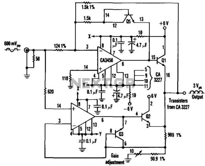
This circuit employs two CA3450 operational amplifiers and a CA3227 transistor array to achieve accurate full-wave rectification of signals up to 10 MHz. Two of the CA3227 transistors are responsible for driving the output, while the other two are...
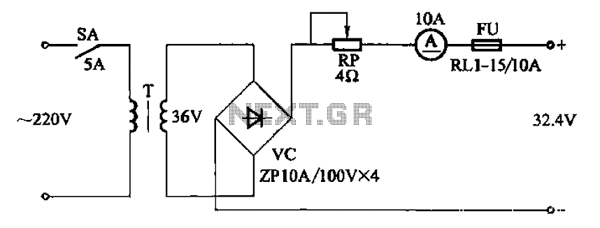
The adjustment potentiometer RP can modify the charging current. The adjustment potentiometer, designated as RP, serves a critical role in regulating the charging current within an electronic circuit. This component is typically a variable resistor that allows for fine-tuning of...
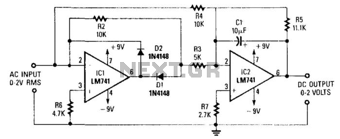
A DC level is generated that corresponds to the AC input RMS value (for a sine wave). The gain of the integrated circuit (IC) is set to a factor of 2 to 1.11. This factor represents the average-to-RMS conversion...
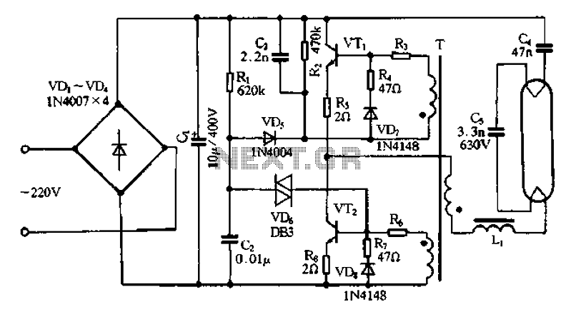
Bridge rectifier circuit in the electronic ballast application circuit The bridge rectifier circuit is a crucial component in electronic ballast applications, primarily utilized for converting alternating current (AC) to direct current (DC). This conversion is essential for powering various electronic...
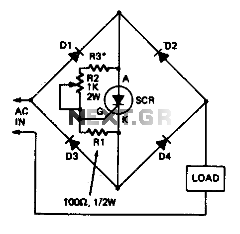
This circuit allows a single Silicon Controlled Rectifier (SCR) to control resistive loads in a full-wave configuration. Resistor R3 must be selected to ensure that when potentiometer R2 is set to its minimum value, the current flowing through the...
A CA3130 BiMOS operational amplifier functions as an attenuator for positive input signals while operating as a conventional operational amplifier for negative input signals. With a 1-V RMS input and a circuit gain of 0.8, its frequency response is...