
H bridge using TPS2836 and CSD16404
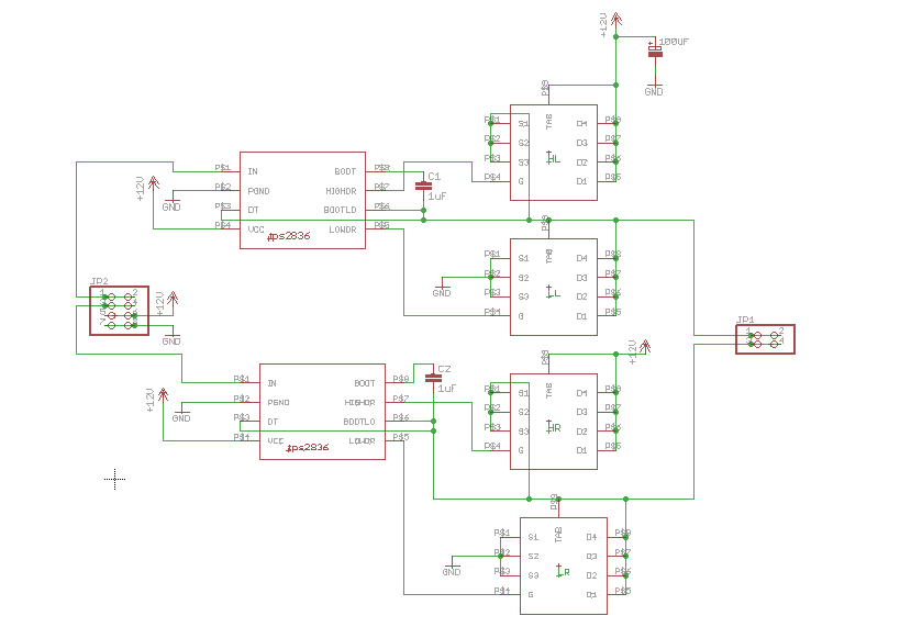
The circuit in question is an H-bridge configuration utilizing the TPS2836 MOSFET driver and CSD16404 MOSFETs. The TPS2836 is designed to drive high- and low-side MOSFETs in a half-bridge configuration, and it requires careful attention to the gate drive voltages to ensure optimal performance. The CSD16404 MOSFET is a N-channel device that requires a gate-source voltage (VGS) of at least 1.8V to turn on effectively, with a recommended minimum of 4.5V for guaranteed Rds(on) performance.
In the described setup, the VDD-GND voltage of 5V is appropriate for powering the TPS2836, but the input signals provided to the MOSFET drivers must be sufficient to ensure that the MOSFETs operate within their specified parameters. The observation that the source voltage of the left high-side MOSFET is 4.5V suggests that the MOSFET is not being fully turned on, as the gate voltage of 5.5V is marginally above the threshold but may not be sufficient for full enhancement, especially under load conditions.
The issue with the right bottom MOSFET showing a drain voltage of 1.5V indicates that it may not be fully turning off or that there could be a fault within the device, possibly due to overheating or damage from soldering. The excessive current draw of 1A when both the right top and left bottom MOSFETs are activated is concerning and suggests that there may be a short circuit or misconfiguration in the circuit.
The TPS2836's floating high-side driver architecture relies on the BOOT capacitor charging to provide the necessary gate drive voltage for the high-side MOSFET. If the low-side MOSFET is not pulsed on initially, the BOOT capacitors (C1 and C2) may not charge adequately, resulting in insufficient gate drive voltage for the high-side MOSFET. It is essential to ensure that these capacitors are within the specified range to avoid startup issues.
In conclusion, a thorough review of the circuit design, including the implementation of the MOSFET drivers, the gate drive voltages, and the presence of any potential faults in the MOSFETs, is necessary to resolve the issues encountered. Additionally, the role of resistors between the driver output and MOSFET gates should be evaluated based on the specific requirements of the application, as they can influence the switching characteristics and performance of the circuit.I made an hbridge using TPS2836 and CSD16404. The schematic is shown below. It does not work properly and I have a few questions about it. It would be great if you can point out where the design is wrong. 1. I gave a VDD-GND of 5V and tried to give the voltages 3. 3V (signifying a logical 1) and 0V (signifying a logical 0) to the inputs of the two mosfet drivers. When I try to turn on the left-high side mosfet, the voltage at it`s source is 4. 5V with no load attached to the driver. The current drawn by the whole circuit is also almost 300 mA. Simultaneously, if the right bottom mosfet is turned on, the voltage at it`s drain is not zero but something around 1. 5V. Note that I am not giving a PWM to the inputs of the mosfet driver but direct voltage levels. Should there be a pulse train coming in to let the charge pump function properly and fully turn on the mosfet The voltage at the gate of left-high mosfet is 5.
5V which is pretty low, when the CSD16404 turns on only at VGS = 1. 8V. 2. If I try to turn on the right top mosfet and the left-bottom mosfet, the whole circuit draws some 1A and things begin to heat up! It could be that the lower-right mosfet is smoked while / after soldering right 3. Are the resistors between the mosfet driver output and the mosfet gate (not used in this circuit) essential for the functioning They are only used to control the turn on times right 1) The CSD16404Q5A must be driven with at least 4.
5 volt Vgs to guarantee the Rds(on) in the on state. The low side MOSFET needs to be pulsed to charge the high side bootstrap circuit with these types of MOSFET drivers. 1. I gave a VDD-GND of 5V and tried to give the voltages 3. 3V (signifying a logical 1) and 0V (signifying a logical 0) to the inputs of the two mosfet drivers. When I try to turn on the left-high side mosfet, the voltage at it`s source is 4. 5V with no load attached to the driver. The current drawn by the whole circuit is also almost 300 mA. Simultaneously, if the right bottom mosfet is turned on, the voltage at it`s drain is not zero but something around 1.
5V. Note that I am not giving a PWM to the inputs of the mosfet driver but direct voltage levels. Should there be a pulse train coming in to let the charge pump function properly and fully turn on the mosfet The voltage at the gate of left-high mosfet is 5. 5V which is pretty low, when the CSD16404 turns on only at VGS = 1. 8V. The TPS2836 driver uses a floating high-side driver. The high-side driver "floats" on the BOOTLO voltage (also called the Switch Node or Phase Node) such that the driver is always seeing the source voltage of the high-side MOSFET.
This driver is powered from the BOOT pin by the BOOTLO to BOOT capacitor (C1 and C2) which are charged through an internal diode through, however if the BOOTLO node is high impedance (low-side drive has not been turned on) the capacitors will not charge properly. It is best to charge these capacitors by turning on the low-side driver (LOWDR) for a short period initially to charge these capacitors.
Note: C1 and C2 are extremely large for this application. This capacitor need only be 0. 1uF - 0. 22uF. Larger capacitors in these locations offer very little benefit, but can slow their initial charge rate and result in start-up issues. 2. If I try to turn on the right top mosfet and the left-bottom mosfet, the whole circuit draws some 1A and things begin to heat up!
It could be that the lower-right mosfet is smoked while / after soldering right It`s possible that the low-side device is damaged. Check the resistance from both BOOTLO pins to GND when the circuit is unpowered. The internal pull-down resistors should force both MOSFETs off, so one would expect several MegOhms of resistance.
3. Are the resistors between the mosfet driver output and the mosfet gate (not used in this circuit) essential for the functioning They are only used to control the turn on times right Gate Driv 🔗 External reference
Related Circuits

The plan for the full bridge inverter circuit involves using IRF2807 MOSFETs (75V Vds, 82A Ids) and two IR2110 driver ICs. Previous attempts to create an H-Bridge for a DC motor were unsuccessful. The DC input voltage is 34V,...
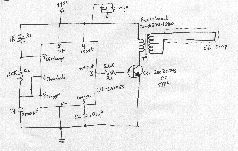
This document outlines a basic circuit designed to power high impedance, high voltage, low current devices such as electroluminescent (EL) backlights and fluorescent tubes. The project originated from the need for a simple yet flexible inverter circuit for an...
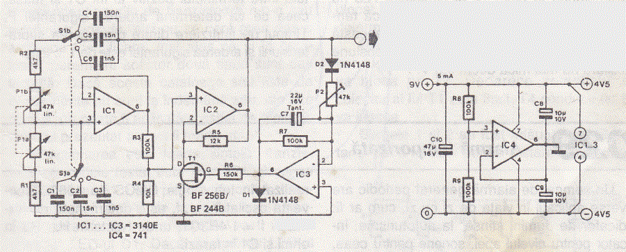
This Wien bridge oscillator is straightforward and, like all Wien oscillators, exhibits low distortion. The resonance frequency can be easily adjusted. The Wien bridge oscillator is a type of electronic oscillator that generates sine waves. It is based on the principle...
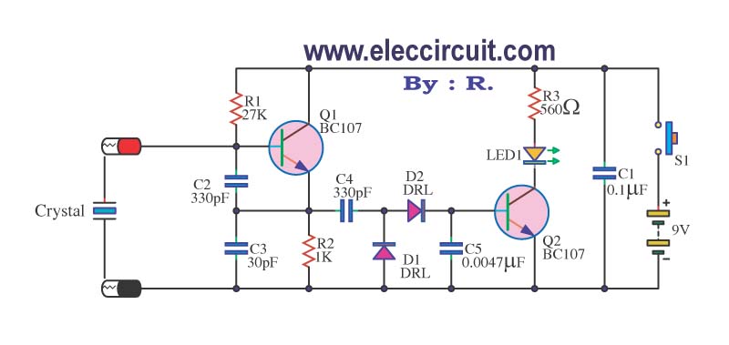
A multimeter cannot be used to test a crystal oscillator. Instead, a dedicated circuit is required, capable of checking crystals within the frequency range of 100 kHz to 900 MHz. This circuit is easy to construct and cost-effective. To construct...
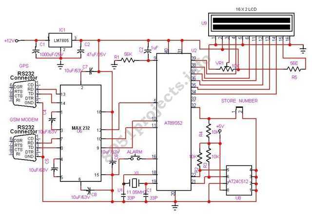
In this project AT89S52 microcontroller is used for interfacing to various hardware peripherals. The current design is an embedded application, which will continuously monitor a moving Vehicle and report the status of the Vehicle on demand. For doing so...

The days of arriving home at night and entering into darkness are finally over. This is a highly practical device, and it has been designed as a module. This device is intended to provide illumination upon entering a dark space,...