
Halogen Lamp Dimmer With Soft Start
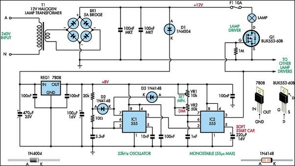
This dimming circuit is designed to enhance the functionality and safety of lighting control in various applications. The use of PWM allows for efficient power modulation, which is particularly beneficial for energy savings and controlling lamp brightness without flicker. The isolation provided by the transformer is crucial for safety, as it prevents high voltage from reaching the low-voltage control circuitry.
The astable 555 timer (IC1) operates as a clock source, generating consistent pulses that trigger the monostable 555 timer (IC2). The variable monostable configuration allows for flexibility in controlling the width of the output pulses, which directly correlates to the brightness of the lamp. The adjustable potentiometer (VR2) provides user control over the dimming range, while the additional potentiometer (VR1) ensures that the circuit can achieve a minimum brightness level.
Diodes D1 and D2 play significant roles in circuit protection and operational integrity, with D1 preventing reverse voltage from affecting the regulator and D2 isolating the timing circuits. The soft-start feature provided by the 220 µF capacitor is particularly advantageous in prolonging the lifespan of lamps, as it reduces the inrush current at power-up, allowing for a gradual increase in brightness.
Overall, this dimming circuit exemplifies a sophisticated approach to lighting control, combining efficient power management with safety features, making it suitable for various lighting applications, including residential and commercial environments. The careful selection of components, such as the BUK553-60A MOSFET and Schottky diodes, ensures reliable performance under varying load conditions.Most dimmers use pulse width modulation (PWM) to control the amount of power that is delivered to the lamp. Those that come bundled with a switch faceplate control the firing angle of a Triac on the 240V mains side.
These work fine with resistive loads but may not be suitable for inductive loads such as low-voltage halogen lamp transformers. This circuit also employs PWM but it switches at a high frequency (22kHz) on the low-voltage side of the lamp transformer. This high frequency also simplifies EMI filtering. Furthermore, because this circuit is isolated from the mains by the transformer, it is relatively safe to build and install.
IC1 is a standard 555 astable oscillator with a high duty cycle. It produces a narrow negative-going pulse at its pin 3 output approximately every 45 µs (ie, the frequency of oscillation is about 22kHz). These pulses trigger IC2, another 555 timer, this time wired as a variable monostable. IC2`s pin 3 output is normally low which means that its internal discharge transistor is on and the 1nF capacitor on pins 6 & 7 is discharged.
However, when the monostable is triggered (by IC1), its output goes high, the internal discharge transistor turns off and the 1nF capacitor charges via VR1 & VR2 until it reaches 2/3Vcc. At this point, the output at pin 3 switches low again. Each time pin 3 of IC2 goes high, it turns on power Mosfet transistor Q1 which in turn switches on the lamp.
Potentiometer VR2 is used to control the time it takes the 1nF capacitor to charge to the threshold voltage and thus sets the width of the output pulses. At maximum resistance, the pulse width is 55ms. This is longer that the 45ms period of oscillator IC1, and so IC2`s pin 3 output is high for 100% of the time and the lamp operates with maximum brightness.
Now consider what happens if the monostable`s period is shorter than the astable`s. In this case, each time IC1`s pin 3 output goes low, pin 7 of IC1 also goes low and discharges IC2`s 1nF timing capacitor via D3. This retriggers the monostable. As a result, IC2 is triggered at a 22kHz rate and produces variable width pulses depending on the setting of VR2.
It`s output in turn pulses Q1 to control the lamp brightness. D2 isolates IC1`s timing circuitry from IC2`s. VR1 is used to set the minimum lamp brightness when VR2 is at minimum resistance. If this control is not required, VR1 can be replaced with a 1. 8kO resistor. The 220 µF capacitor on pin 5 of IC2 provides a soft-start facility to prolong lamp life. Initially, when power is first applied, the 220 µF capacitor is discharged and this lowers the threshold voltage (which is normally 2/3Vcc). That in turn results in shorter pulses at the output. As the 220 µF capacitor charges, the threshold voltage gradually increases until the circuit operates "normally".
For the prototype, Q1 was a BUK553-60A, rated at 60V, 20A & 75W. Q1`s maximum on-state resistance is 0. 1O, so switching a 4A lamp load results in a maximum power dissipation of 1. 6W. The bridge rectifier comes in at around 5W and so both should be mounted on suitable heatsinks. The power dissipation in the bridge rectifier can be reduced by using power Schottky diodes rated at 5A or more. The output of 555 timer IC2 is capable of directly driving several Mosfets (up to four in tests). Note, that if the Mosfet is going to be some distance from the 555, it will be necessary to buffer it.
Power for the control circuitry is derived from 3-terminal regulator REG1 which produces an 8V rail. This in turn is fed from the output of the bridge rectifier via diode D1 🔗 External reference
Related Circuits
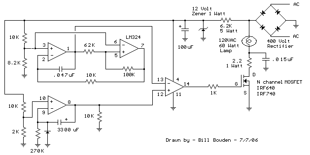
This circuit gradually illuminates a 120VAC lamp over an approximate 20-minute period. A bridge rectifier converts the AC voltage to 120V DC, supplying power to the MOSFET and the 60-watt lamp. A 6.2K, 5-watt resistor along with a Zener...

This simple circuit can be used to flash incandescent lamps with a power rating of up to 10W. It is ideal for creating flashing beacons on automobiles and similar applications. The circuit consists of an astable multivibrator utilizing transistors...
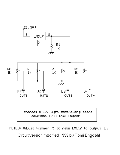
This circuit is a simple manual analog light control desk that outputs standard 0-10V control signals suitable for controlling professional light dimmers and other lighting equipment. The controller's output is a steady DC voltage that varies between 0 and...
The image 3-6 depicts a thermistor temperature or frequency conversion circuit. The resistance of thermistors changes linearly with temperature, allowing this change to be utilized in a voltage-controlled oscillator. In the circuit, operational amplifiers A1-A4 are current-type LM3900 models,...
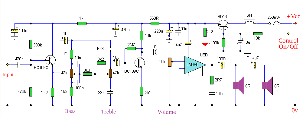
Amplifier with tone controls and soft switching. Notes: The soft switching is enabled by a BD131 transistor configured as a switch in an emitter follower arrangement. The collector is connected to a permanent load. The described amplifier circuit incorporates tone...
.jpg)
The HID ballast circuit consists of a buck stage for regulating lamp current and power, a full-bridge output stage that generates a low-frequency (200Hz) AC square-wave voltage and current to drive the lamp, and an ignition circuit that produces...