
Creating an HID Ballast with Constant Lamp Power Control
.jpg "Creating an HID Ballast with Constant Lamp Power Control")
The HID ballast circuit is designed to efficiently drive high-intensity discharge (HID) lamps, ensuring optimal performance and longevity. The buck stage is critical for converting the high input voltage (400VDC) into a controlled output that maintains the necessary current for the lamp operation. The buck converter topology enables efficient energy conversion, minimizing losses and heat generation.
The full-bridge output stage is responsible for generating the square-wave AC signal, which is essential for operating HID lamps. The 200Hz frequency is specifically chosen to match the requirements of the HID lamp, allowing for effective light output while minimizing flicker. The external timing control (CT pin) allows for flexibility in adjusting the frequency, catering to various lamp specifications and operational conditions.
Power management within the circuit is achieved through precise sensing of both voltage and current at the lamp. The VSENSE and ISENSE pins provide real-time feedback to the IC, which employs an internal multiplication process to calculate the power delivered to the lamp. This feedback loop is crucial for maintaining lamp power stability, particularly in varying load conditions, ensuring consistent light output and preventing damage to the lamp due to overcurrent situations.
The ignition circuit is designed to deliver high-voltage pulses necessary for starting the HID lamp. The timing control provided by the IGN pin allows for the ignition sequence to be optimized for different lamp types, ensuring reliable ignition under varying conditions. The components associated with the ignition circuit (MIGN, DIGN, CIGN, TIGN) work together to create the required pulse sequence, facilitating the lamp's transition from a non-operational to an operational state.
The inclusion of a programmable fault timer (TCLK pin) enhances the safety and reliability of the ballast circuit. By monitoring various fault conditions, the IC can proactively manage potential issues such as lamp failure or instability. This feature is particularly important in applications where lamp failure could lead to significant operational disruptions, allowing for timely shutdown and protection of both the circuit and the lamp.
Overall, the HID ballast circuit represents a sophisticated solution for driving HID lamps, integrating advanced control features, safety mechanisms, and efficient power management to ensure optimal performance and reliability.The HID ballast circuit includes (Figure 1) a buck stage for controlling lamp current and power, a full-bridge output stage for driving the lamp with a low-frequency (200Hz), AC square-wave voltage and current, and an ignition circuit for producing 4KV peak voltage pulses to ignite the lamp. The input to the buck stage is a constant 400VDC voltage that is typically supplied by a standard PFC boost circuit.
The operating frequency of the full-bridge is controlled with an external timing pin (CT pin). The IC provides lamp power control by sensing the lamp voltage and current (VSENSE, ISENSE pins), multiplying them together internally to generate the lamp power measurement, and then steering the buck on-time to keep the lamp power constant. The ignition control is performed using an ignition timing circuit (IGN pin) that drives the ignition circuit of the lamp (MIGN, DIGN, CIGN, TIGN) on and off at a set interval (TIGN pin).
Finally, the IC includes a programmable fault timer (TCLK pin) for programming the allowable fault duration times before shutting the IC off safely. Such fault conditions include failure of the lamp to ignite, failure of the lamp to warm-up, lamp end-of-life, arc instability, and open/short circuit of the output.
🔗 External reference
Related Circuits

A laptop computer power supply that provides a 9-V output, includes crowbar overvoltage protection, and operates from a 12-V input supply is described. The input supply voltage must be at least 3.6 V above the desired output voltage. The...
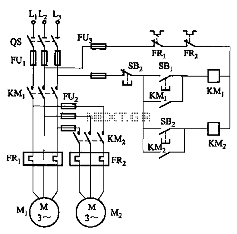
The circuit illustrated in Figure 3-83 demonstrates that the contactor KMi is activated only after it is pulled, which indicates that the motor Mi has started for the first time. Following this, the contactor KM2 is then activated, indicating...
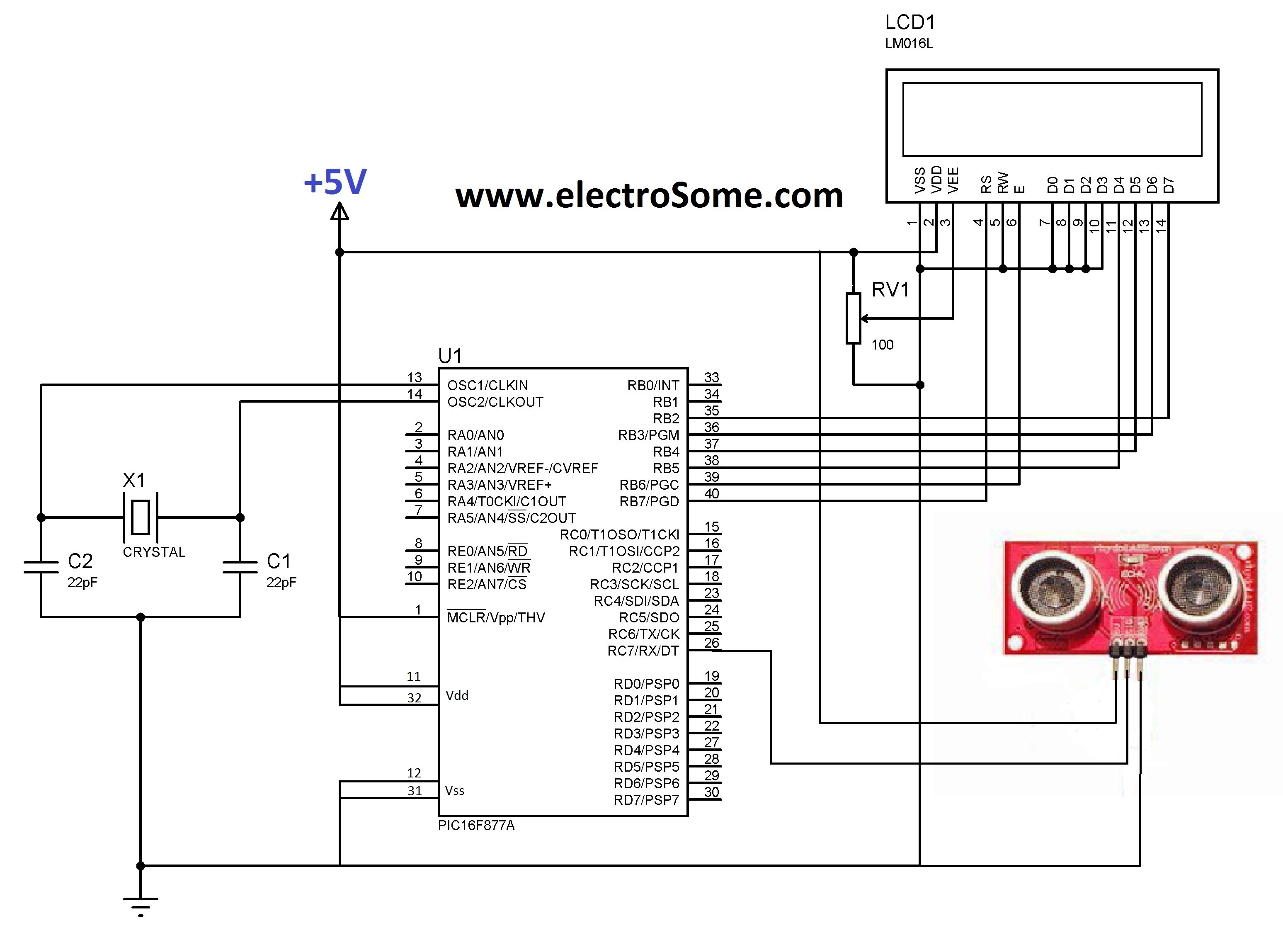
LCD initializations in 8051 C programming involve understanding the logic behind serial communication, including the duration of SIG pulse transmission and the necessary delays. These statements inform the compiler that a 16x2 LCD is connected to the defined pins...
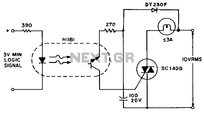
A simple solid-state relay circuit drives the 10-Vac telephone indicator lamps from logic circuitry while maintaining complete isolation between the 10-V line and the logic circuit. The described circuit utilizes a solid-state relay (SSR) to control 10-Vac telephone indicator lamps...
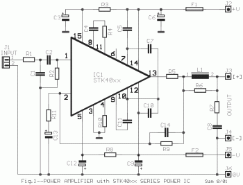
This is a power audio amplifier circuit based on the STK400xx series. It provides high-quality sound and is cost-effective, as the STK40xx series is affordably priced. The circuit can be easily constructed using only a few external components. The...
The W7800 is a positive integrated voltage regulator, while the F007 consists of an operational amplifier used in a power supply tracking application circuit. Some configurations utilize both positive and negative power supplies, with a negative supply necessary to...