
Handheld Oscilloscope Oscillator Circuit

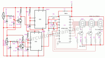
The infrared transmitter circuit operates by generating a modulated infrared signal that can be detected by a compatible receiver. The core components involved in this process include transistors T1, T2, and T3, which function as switches and amplifiers, and the passive components R1, R2, C1, and C2, which set the timing and frequency of the oscillation.
Transistor T1 is responsible for initiating the oscillation process. When T1 is turned on, it allows current to flow through the circuit, charging capacitor C1. The charging of C1 is critical as it influences the timing characteristics of the circuit. Once C1 is charged, it creates a voltage across it, which subsequently drives the base of transistor T2. The configuration of R1 and R2 determines the rate at which C1 charges and discharges, thus directly affecting the frequency of the oscillation.
Transistor T2 serves to further modulate the signal, with its output driving the base of T3. The interaction between T1 and T2 creates a feedback loop that sustains the oscillation. The output from T3, which is the final stage of the transmitter, generates the pulsed infrared signal that is emitted through the infrared LEDs.
The values of R1 and R2 primarily dictate the charge and discharge time constants of C1, while C2 can influence the stability and frequency of the oscillation by providing additional capacitance in the circuit. By adjusting these component values, the designer can fine-tune the frequency of the emitted infrared signal to match the requirements of the application, ensuring effective communication between the transmitter and the receiver.
Overall, the infrared transmitter circuit exemplifies a straightforward yet effective design for wireless communication, leveraging fundamental electronic components to achieve the desired functionality.The circuit in the schematic below is an infrared transmitter. The infrared beam is transmitted in a nearly line-of-sight pattern to another device with an infrared receiver. The plotted waveforms are the output voltages of the two intermediate stages (purple and yellow) and the transmitter`s output stage (green).
To measure the voltage pulsed acr oss the transmitting IR LEDs, use iMSO-104`s analog input as a traditional oscilloscope. Clip the ground clamp to a suitable anchor point on the circuit, and attach the scope probe lead to the collector leg of transistor T3, as indicated with a green dot in the schematic. The voltage oscillations of T1 and T2, purple and yellow respectively, drive the base voltage of T3 and create the pulsed output.
Capacitor C1 only charges when T1 is turned on and conducting, and T2 is turned off with its base voltage pulled high (meaning that the base voltage is essentially the same as the supply rail voltage) The oscillation frequency is set by the values of four components: R1 and R2, and C1 and C2. There are two ways that these component values affect the frequency. 🔗 External reference
Related Circuits

The circuit depicted is a single-phase bridge rectifier. It consists of arms with a cathode (negative electrode) and parallel anodes (positive electrodes) arranged in a configuration that connects multiple rectifier modules to form a bridge, commonly referred to as...

Using a Thomson TEA2025, this stereo amplifier delivers 1 W per channel into a 4-ohm load with a 9-V supply. The input sensitivity is 25 mV peak-to-peak for full output. It is important to ensure that pins 4, 5,...
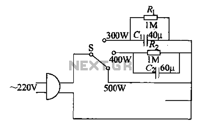
Each family has essential small appliances. The sub-type is an electric power jet, mainly used for clothes and hot shaping. The iron's circuit is shown in Figure 1-30. When using an iron, there is always a concern about using...
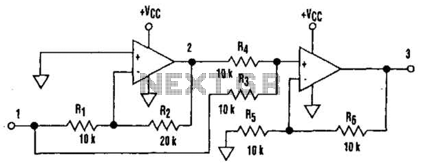
It is well understood that utilizing single-supply operational amplifiers (op amps) can present challenges when implementing simple functions in a bipolar signal environment. Often, this necessitates the use of additional op amps and other electronic components. Considering this, it...
This room light controller project automatically uses a microcontroller to manage a visitor counter, providing a reliable circuit for controlling the room lighting. The room light controller circuit integrates a microcontroller that processes inputs from a visitor counter. This setup...
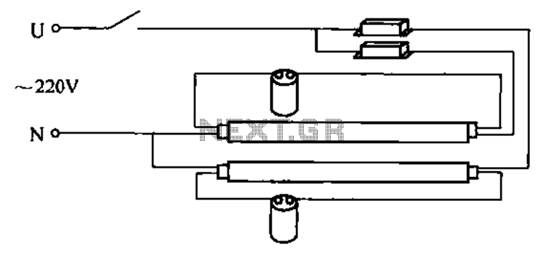
A double tube fluorescent lighting circuit is illustrated. In certain situations, a single tube light may not fulfill the lighting requirements, necessitating the use of double tube lighting. The physical installation is depicted in the circuit of a double...