
hf 5 band mosfet amplifier
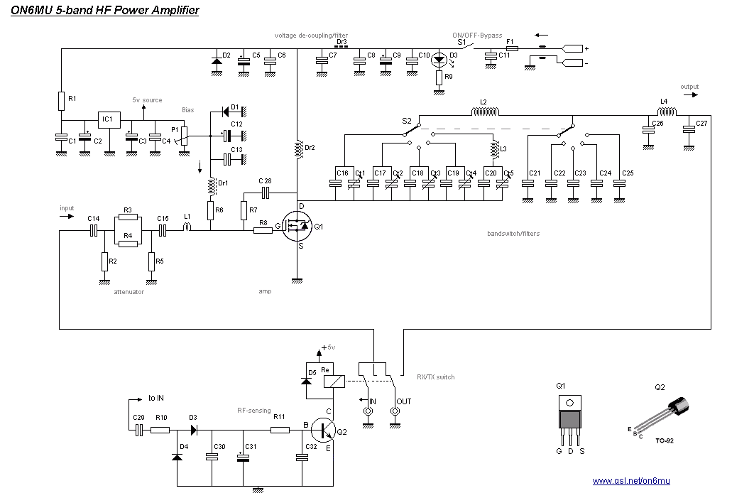
The IRF510 MOSFET is a key component in this power amplifier design. Its operation as an N-channel enhancement mode device allows for efficient amplification of RF signals. The high input impedance characteristic of the MOSFET minimizes loading on the preceding stages, thus preserving signal integrity. The biasing method employed ensures that the MOSFET operates within its linear region, which is crucial for maintaining signal fidelity.
The integration of the T-R relay enhances the functionality of the amplifier by providing seamless transition between transmit and receive modes. This relay is sensitive to RF signals, ensuring that the amplifier is engaged only during transmission, thereby preventing unnecessary power consumption and potential damage during reception.
The choice of an L-filter for impedance matching is particularly relevant in RF applications, as it provides a simple yet effective means of ensuring maximum power transfer to the antenna. This method is favored for its ability to minimize reflections and losses that can occur at the interface between the amplifier and the antenna.
The performance limitations associated with the IRF510, particularly regarding frequency response and output linearity, are acknowledged. Careful consideration is given to the design to mitigate these challenges, including potential adjustments to the circuit to optimize performance across multiple bands. The design ethos prioritizes versatility and simplicity, allowing users to operate across various frequency bands while managing the trade-offs inherent in such a configuration.
The overall design of this power amplifier, with its combination of modern MOSFET technology and traditional impedance matching techniques, represents a thoughtful approach to amateur radio amplification, catering to the needs of operators seeking a reliable and effective solution for RF transmission.This project uses a widely available IRF510 MOSFET. This N-Channel enhancement mode silicon gate power field effect transistor is an advanced power MOSFET designed, tested, and guaranteed to withstand a specified level of energy in the breakdown avalanche mode of operation. MOSFETs operate very differently from bipolar transistors. MOSFETs are vol tage-controlled devices and exhibit a very high input impedance at dc, whereas bipolar transistors are current-controlled devices and have a relatively low input impedance. Biasing a MOSFET for linear operation only requires applying a fixed voltage to its gate via a resistor.
The built-in self-regulating actions prevent MOSFETs from being affected by thermal runaway. MOSFETs do not require negative feedback to suppress low-frequency gain as is often required with bipolar RF transistors. I chose the IRF510 because lots of hams use `em and they`re cheap. But they perform a bit less when it comes to constant gain and/or power output across a wide range of frequency bands.
I wasn`t especially concerned with that, and the advantages outweigh the contra`s, so I went with that MOSFET. Rather then using a 1:4 toroid (which is excellent) to match Q1 impedance to 50 Ohms, I have applied the "old school" radio valve coupling; impedance matching circuitry between the output and the antenna using a L-filter.
Why FET devices are more closely related to vacuum tubes than are bipolar transistors (and because I do like to do things my way HI). Both vacuum tubes and the FET are controlled by the voltage level of the input rather then the input current.
They have three basic terminals, the gate, the source and the drain. These are related and can be compared to the vacuum tube terminals. The ralationship between the two doesn`t stop here. The two most important relationships are called the transconductance and output. An advantage of MOSFET devices is that they do not have gate leakage current and MOSFETs do not need input and reverse transconductance. The amplifier is made to be driven by transmitters in the ½ to 2 watt range. Built-in to the power amplifier is a sensitive (Q2) T-R relay which will switch the unit in and out of the antenna line.
When in receive, the amplifier is bypassed and the antenna feeds directly to the input jack, when you go to transmit, the T-R circuit detects the transmit RF power and automatically switches the power amplifier into the circuit and amplifies the applied RF power. If you decide to run "barefoot" turning off the AMP it will disable the amplifier and your QRP The input drive can be anything from 0.
4watt to 2 watt max, which will be amplified to +/- 25 watt. The output varies on the drive power and the applied voltage. The power output is not perfectly linear to the input frequency/band. The impedance 50 Ohms match could be solved by using a 1:4 toroid, or as I like to use, the "old school" radio valve coupling; impedance matching circuitry between the output and the antenna using a L-filter. And, the IRF510 isn`t perfect (note: there are also low grade versions of the Mosfet out there which can lower the output power and influence the quality of the signal/waveform).
The N-channel mosfet has an input capacitance thats a bit on the high side and the output capacitance that varies with the cross over frequency. It can be a slight problem when it comes to constant gain and/or power output across a wide range of frequency bands.
I wasn`t especially concerned with that so I went with this MOSFET anyway. Of course the main issue was the simple design to be able to use one band or even up to five bands if wanted, which always has some compromise in this type of design. This means that there is some fluctuation of the output power par band. When driven between the optimal range of +/- 1. 5 watt the amplifier more then capable to deliver 25 watts +/- 10%. Output power for AM should be set to +/- 50% of max. 🔗 External reference
Related Circuits
LM3876-based 50-watt audio amplifier circuit. Operates from +/-35V DC. Simple design, low noise. The LM3876 is a high-performance audio power amplifier designed for driving speakers in various audio applications. This particular circuit configuration enables the amplifier to deliver up to...
The LM2002 / 2002A is an audio power amplifier integrated circuit. The LM2002A features high voltage protection, with a maximum instantaneous power supply voltage of up to 40V, and comes in a 5-pin single in-line plastic package. This integrated...
When the power supply reaches the circuit and the input signal is applied, the sound signal is processed through capacitor C1 and resistor R1 for signal coupling and noise reduction. The modified signal then reaches pin 3 (non-inverting) of...
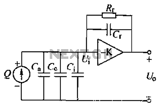
A charge amplifier is an effective device for measuring punch hits. This amplifier utilizes a negative feedback capacitor in conjunction with a high-gain operational amplifier. The amplifier operates with minimal shunt, relying primarily on the feedback capacitor's charge (q...
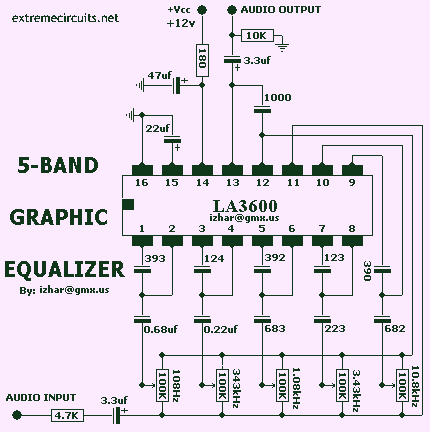
This complete high quality, low noise 5-BAND GRAPHIC EQUALIZER circuit is based around Monolithic Linear integrated circuit LA3600 manufactured by SANYO. This circuit is very easy to build and has good Quality. You can use it with Portable component...

A series of active RF filters using the National LM3481C comprises a ten-band graphic equalizer. C1, C2, R1, and R2 should be at least 10% with 5% preferred tolerances. The circuit design features a ten-band graphic equalizer that utilizes a...