
HF phone rig for 20-40 meter band
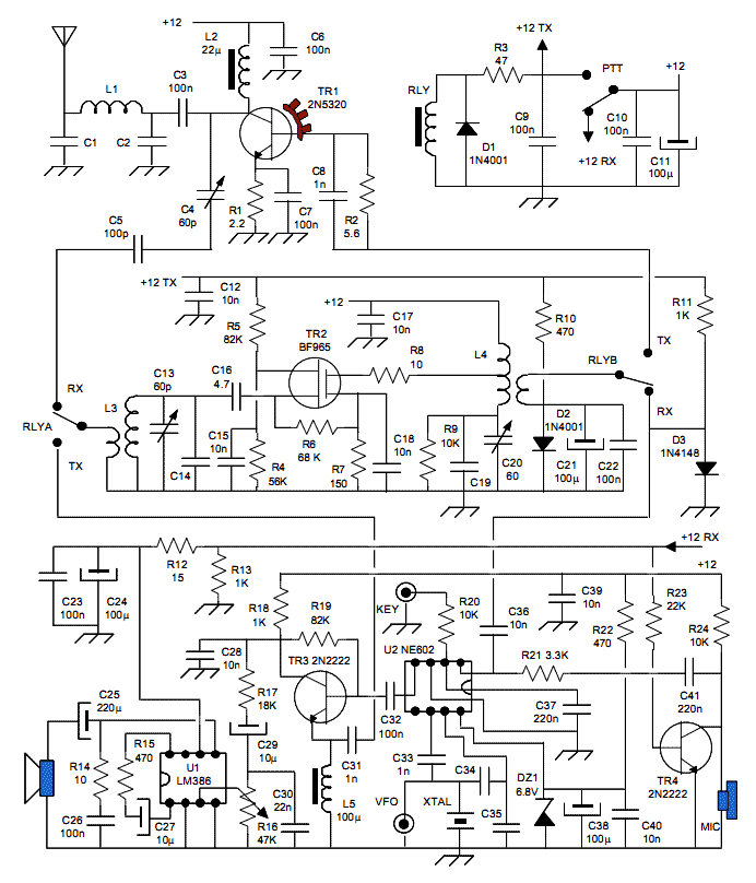
The described circuit represents a straightforward yet effective design for a portable DSB (Double Sideband) transmitter and receiver, suitable for amateur radio enthusiasts. The architecture features a direct conversion receiver that utilizes a BF965 MOSFET as the initial amplification stage, providing a gain of approximately 10 dB. This is followed by a product detector implemented with an NE602 IC, which further amplifies the signal by 18 dB. The use of a variable capacitor (C4) allows for fine-tuning of sensitivity, enabling optimal performance in the presence of strong adjacent signals.
The audio output from the receiver is processed through a 2N2222 transistor and an LM386 audio amplifier, which drives an 8-ohm speaker, delivering sufficient audio power for clear sound reproduction. The design emphasizes low power consumption and compact dimensions, making it highly portable.
For the transmitter section, the NE602 is also employed as a balanced modulator, with an additional 2N2222 transistor functioning as an emitter follower to boost the signal. The BF965 MOSFET acts as a driver stage, producing output levels of 30-40 mW. The final amplification stage utilizes a 2N5320 transistor, configured with a Pi filter to smooth the output, resulting in a total output power of approximately 1.5 W.
The TX/RX functionality is managed by a PTT (Push-To-Talk) switch, which controls the operation of a micro relay to switch between transmitting and receiving modes. This relay configuration ensures that the MOSFET amplifier can function effectively in both modes without causing interference. The gain and power levels in the transmitter are regulated by a resistor (R5) connected to the gate of the MOSFET, preventing overload during reception.
The circuit can be adapted for either fixed frequency operation using a crystal or variable frequency operation via a VFO (Voltage Controlled Oscillator), providing flexibility for different user needs. The PCB design accommodates both configurations, ensuring ease of assembly for homebrewers. Overall, this project exemplifies a practical approach to building a compact and efficient DSB communication rig.A simple project, within most of homebrewers capabilities. Very simple tuning, a single stage to align, besides VFO frequency adjusting. Easy to find, cheap components. Reduced dimensions and low power requirement, a totally portable rig. It's worth while to spend some words about the DSB modulation. It's simply a type of amplitude modulation (AM). It is common knowledge that an AM signal is composed by a carrier and two sidebands, wich take the whole information. The figure below represents an AM signal at 14.000 KHz, modulated with a 5 KHz bandwide BF signal. The receiver is a direct conversion unit. It is composed by a double tuned preselector, equipped with a BF965 mosfet, delivering a 10 dB gain, and a product detector using a "classic" NE602 (2) (further 18 dB of gain). A variable capacitor C4 allows to adjust the sensitivity according to the connected antenna, so we may find a right compromise to limit the effects of the strong broadcastings operating at the band edges.
The detected audio is amplified by a 2N2222 transistor and an LM386 (3) IC delivering a few hundreds mW into an 8 Ohm speaker. RLYA MIC +12 +12 PTT +12 +12 TX RLY VFO U2 NE602 U1 LM386 RX RX TX +12 RLYB +12 TX TX TR2 BF965 TR1 2N5320 C41 220n C33 1n DZ1 6.8V C38 100m C40 10n C37 220n R24 10K C36 10n C24 100m C23 100n C25 220m R14 10 C26 100n R17 18K C30 22n C29 10m C31 1n L5 100m R18 1K R19 82K R4 56K R5 82K R6 68 K R7 150 C16 4.7 D1 1N4001 R22 470 R10 470 C27 10m R15 470 XTAL C1 C2 L1 L2 22m C6 100n C4 60p C7 100n R1 2.2 C8 1n R2 5.6 R3 47 C9 100n L3 C13 60p C14 C15 10n +12 RX +12 RX R23 22K TR4 2N2222 C11 100m C10 100n C17 10n C18 10n C19 C20 60 C21 100m C22 100n L4 C5 100p C32 100n C34 C35 R9 10K R13 1K KEY R20 10K C3 100n R8 10 TR3 2N2222 R16 47K D2 1N4001 R21 3.3K R12 15 C28 10n R11 1K D3 1N4148 C12 10n C39 10n RLYA MIC +12 +12 PTT +12 +12 TX RLY VFO U2 NE602 U1 LM386 RX RX TX +12 RLYB +12 TX TX TR2 BF965 TR1 2N5320 C41 220n C33 1n DZ1 6.8V C38 100m C40 10n C37 220n R24 10K C36 10n C24 100m C23 100n C25 220m R14 10 C26 100n R17 18K C30 22n C29 10m C31 1n L5 100m R18 1K R19 82K R4 56K R5 82K R6 68 K R7 150 C16 4.7 D1 1N4001 R22 470 R10 470 C27 10m R15 470 XTAL C1 C2 L1 L2 22m C6 100n C4 60p C7 100n R1 2.2 C8 1n R2 5.6 R3 47 C9 100n L3 C13 60p C14 C15 10n +12 RX +12 RX R23 22K TR4 2N2222 C11 100m C10 100n C17 10n C18 10n C19 C20 60 C21 100m C22 100n L4 C5 100p C32 100n C34 C35 R9 10K R13 1K KEY R20 10K C3 100n R8 10 TR3 2N2222 R16 47K D2 1N4001 R21 3.3K R12 15 C28 10n R11 1K D3 1N4148 C12 10n C39 10n3 The transmitter employs the same NE602 as a balanced modulator, while TR3 (2N2222) acts as an emitter follower.
The mosfet stage is now employed as a driver, with an adequate voltage applied to the gate 2, so as to raise the output signal level up to 30-40 mW. The final stage is equipped with a common 2N5320, followed by a simple Pi filter. The output power is about 1,5 W. Notice that the L2 inductor must bear the final stage current (about 200 mA) with a little voltage drop, so do not use a too little component.
The mike is a fet preamplified unit, TR4 inhibits its working while in RX mode. The TX/RX switching system uses a PTT mechanical switch wich delivers the supply voltage to RX / TX sections and drives a two exchanges micro relay. The relay switches the input and output lines in the mosfet amplifier, so allowing its double function.
Notice that the mosfet's gain and power delivery are controlled by the R5 resistor on gate 2, applying the control voltage only in TX mode. So doing we can avoid overloading of the NE602 mixer in RX mode, limiting annoying interferences from broadcasting.
The same voltage biases the D3 diode so as to inhibit RF signal from reaching the balanced modulator input. The RIG may be built in two versions : - Fixed frequency, using a crystal cut to the desired frequency (a cheap 14.318 KHz computer crystal may be used for 20 m band).
In this version C34 and C35 capacitors, both 47 pF value, must be mounted. - VFO driven (description follows in the next chapter). In this case only C35 capacitor, 1 nF value, must be mounted. the PCB board is suited to both versions. 🔗 External reference
Related Circuits
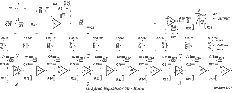
The provided description pertains to a graphic equalizer, a device used for selectively attenuating or boosting specific frequency bands in an acoustic spectrum. This function allows for the adaptation of musical reproduction to the acoustics of a particular space. However,...
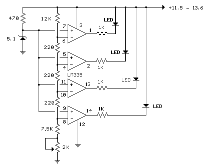
The circuit utilizes a quad voltage comparator (LM339) as a basic bar graph meter to display the charge status of a 12-volt lead-acid battery. A 5-volt reference voltage is applied to each of the positive (+) inputs of the...
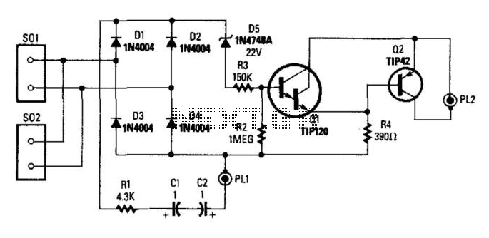
This circuit controls a tape recorder through PL2. When the phone is on-hook, D5 conducts, activating Q1 and disabling Q2. Additionally, ringing voltage will also trigger D5 to conduct; C2 and C1 should be rated for 150 V or...
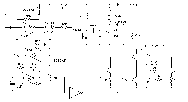
The telephone ring generator shown below generates the needed high voltage from a simple switching mode power supply (SMPS) which employs a CMOS Schmitt Trigger square wave oscillator, 10 mH inductor, high voltage switching transistor (TIP47 or other high...
This circuit initiated the development of various Link Telephone Intercom designs. Originally created in 1996 using heavy-duty relays and contact banks, it was updated last year to incorporate IC1 in place of a simpler transistor multivibrator. All relays and...
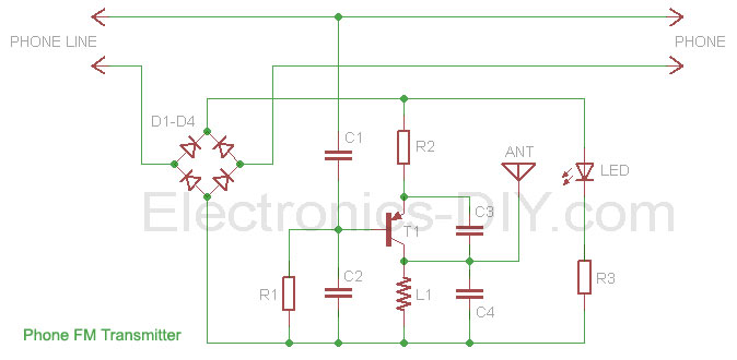
This phone FM transmitter connects in series to a telephone line and transmits telephone conversations over the FM band when the telephone handset is picked up. The transmitted signal can be tuned by any FM receiver. The circuit includes...