
High-frequency signal output amplifier
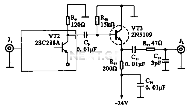
The described circuit utilizes a common collector configuration, also known as an emitter follower, to achieve impedance matching and provide a high input impedance while maintaining a low output impedance. This configuration is particularly beneficial in high-frequency applications, as it minimizes signal distortion and maximizes bandwidth. The VI3 amplifier is specifically tailored for high-frequency operations, capable of handling frequencies ranging from 1 MHz to 250 MHz, making it suitable for a variety of communication and signal processing applications.
The output stage of the circuit is designed to amplify the voltage signal while ensuring that the power output is significantly increased. This is crucial for applications requiring strong signal transmission over longer distances or through lossy mediums. The use of a negative power supply enhances the performance of the amplifier by allowing for a wider dynamic range and improved linearity, which is essential in high-frequency signal amplification.
In this specific design, the emitter follower configuration allows for the direct application of the output from the high-frequency wideband amplifier (VT3) to the base of the common collector amplifier. This connection facilitates efficient signal transfer and minimizes losses, ensuring that the high-frequency characteristics of the signal are preserved. Additionally, the circuit is optimized for low noise operation, which is a critical factor in high-frequency applications where signal integrity is paramount.
Overall, the combination of a common collector amplifier with a negative power supply and high-frequency design principles results in a robust circuit capable of delivering enhanced performance in various electronic applications.A high frequency signal is shown in the output amplifier, the circuit is constituted by a VI3 common collector amplifier (emitter follower), in order to improve the child-band high-frequency amplifier (1-250 MHz) of the output voltage, increasing the power output stage circuit. This circuit uses emitter, a signal from the high-frequency wideband amplifiers, VT3 applied to the base of the circuit with the first stage of a wideband high frequency amplifier, are performed using negative power supply, thus improving pre-wideband high-frequency amplifier capacity.
Related Circuits
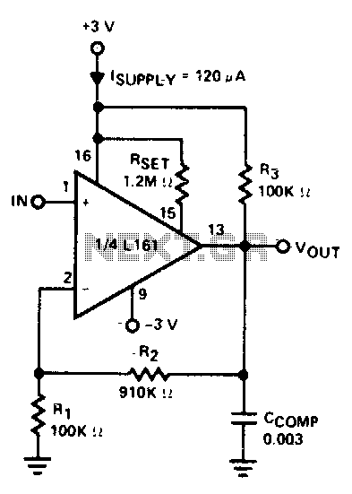
The amplifier is 3 dB down at 100 kHz and has a slew rate of 0.02 V/µs. The amplifier's performance characteristics indicate that it experiences a 3 dB attenuation at a frequency of 100 kHz. This specification suggests that at...
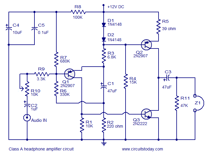
Transistor amplifier circuits that are simple and easy to construct. This includes a headphone amplifier, a four-transistor amplifier, and a low-power amplifier. Transistor amplifier circuits are fundamental components in electronic design, offering various applications ranging from audio amplification to signal...
This article discusses low dropout voltage regulator circuits (LF353DRG4). The content is straightforward and informative. The components mentioned in this article can enhance understanding of the topic. For instance, readers can find and purchase components like LF353DRG4. The article...
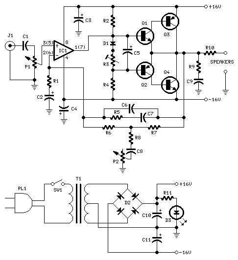
This design is based on an 18 Watt audio amplifier and was developed primarily to meet the needs of users who are unable to find the TLE2141C chip. It utilizes the widely available NE5532 dual integrated circuit; however, its...
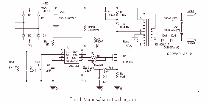
A high voltage step-up DC power supply using adjustable flyback conversion. The described circuit is a high voltage step-up DC power supply that employs an adjustable flyback converter topology. Flyback converters are widely used in applications requiring electrical isolation and...
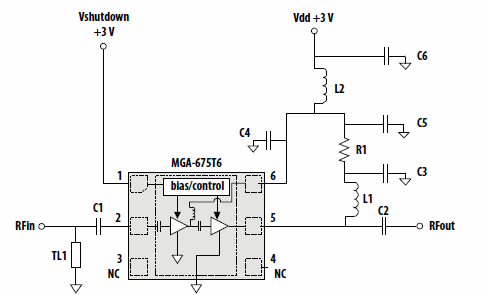
This application note discusses the use of Avago Technologies' MGA-675T6 for 5-6 GHz applications. The MGA-675T6 is internally integrated with shutdown and biasing circuitry, which simplifies the external circuitry. The shutdown feature allows the low noise amplifier (LNA) to...
Warning: include(partials/cookie-banner.php): Failed to open stream: Permission denied in /var/www/html/nextgr/view-circuit.php on line 713
Warning: include(): Failed opening 'partials/cookie-banner.php' for inclusion (include_path='.:/usr/share/php') in /var/www/html/nextgr/view-circuit.php on line 713