
High-performance DC amplifier driving circuit AP500A-01
The AP500A amplifier is designed to cater to a variety of audio amplification needs, making it an ideal choice for high-fidelity audio systems. The versatility in amplifier configuration allows for tailored applications based on specific user requirements. The use of VMOS FET technology provides a modern solution to traditional tube amplification, combining the warmth of tube sound with the efficiency of solid-state devices.
The circuit design, as depicted in the provided figures, emphasizes a robust architecture that supports both voltage and current amplification, ensuring that the amplifier can deliver high output power while maintaining audio quality. The adjustable resistor feature allows for fine-tuning of the amplifier's performance, accommodating different types of audio signals and speaker configurations.
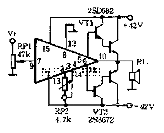
Moreover, the inclusion of auxiliary radiator fins is a critical consideration in the design, as it addresses thermal management, which is vital for maintaining the longevity and reliability of the amplifier under high load conditions. The ability to operate within a wide voltage range enhances the AP500A's adaptability, making it suitable for various power supply scenarios without compromising performance. This makes the AP500A a highly effective and efficient solution for audio amplification in both professional and consumer applications. Because so many AP500A having the above advantages, the use to which the stereo has incomparable superiority. AP500A use can be made of OTI, ) CI a, rK, BTL, class AB, super CP I, CPI and other distinctive © amplifier circuit shown in Figure 3-21, Figure 3-22 is AP500A the typical DC amplifier module using a circuit diagram 6 wherein AP500A amplifier for voltage amplification and drives VT1, VT2 amplifier tube, VT1, VT2 as amplifier current amplification tasks Figure 3-22 uses VMOS FET amplifier tube, having an electron tube characteristics VM () S tube amplifier with DC FET input AP500A equipped with, can fully play VMOS tube Ix, amplifier unique treble slim, powerful bass special point © Figure 3-23 is present amplifier power supply circuit, FIG. 3 -21 3-22 when using 42V power supply, output power up to 2, oow when 2 port power supply with disabilities 28V, 90W 2 can output power ratio.
Since AP500A extremely wide voltage adaptability, so recommended within the operating voltage range ( 4zv including, 28V), the circuit can work without debugging port working status amplifier tube stringent requirements, according to FIG. 3 21, Figure 3-22 adjustable resistor connected in dotted line shown to set the end of the longevity amplifier tube VTl.VT2 working condition (eg; B, AB or class a class can also be connected to a small auxiliary element in the peripheral circuit, so VTlVT2 enter the working state super CPI) port Further, since the power amplifier tube amplifier for the last stage is a current amplification, large power consumption, so the need to use an auxiliary radiator fins.
Related Circuits
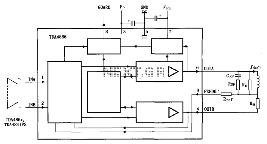
The TDA4866 is a 90-color power amplifier designed for vertical deflection systems, operating at a frequency range of 50 to 160 Hz. The CRMM circuit is implemented to ensure a high current drive input. The amplifier features a dual...

This is a circuit for an accelerometer amplifier. It is a straightforward circuit. A precision accelerometer requires an inverting mode amplifier since these devices typically output charge. This amplifier converts charges into a voltage output. The circuit presented below...
Last year, a low-cost tube stereo headphone amplifier kit from Oatley Electronics (located in New South Wales, Australia) was built and reviewed. This kit gained significant popularity and was sold globally. The headphone amplifier is based on new old...
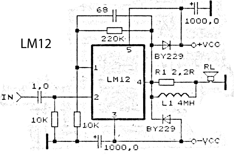
This is an amplifier circuit utilizing the LM12 integrated circuit as the primary amplifier. The amplifier delivers a power output of 150 watts and operates with a load impedance of 4 ohms. It is classified as a high-output power...
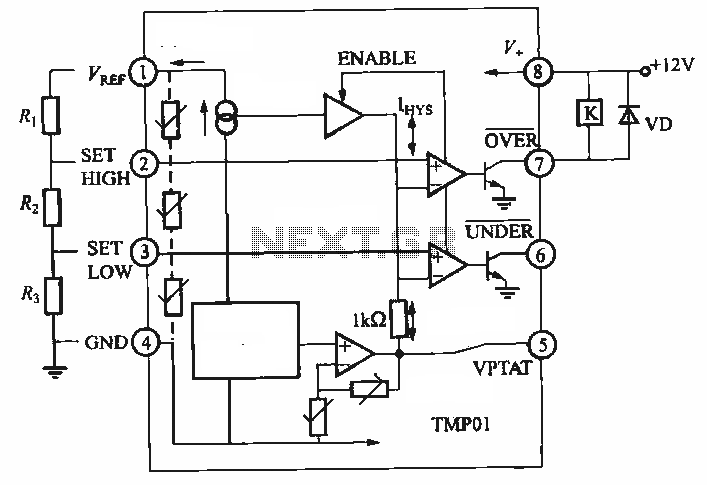
TMP01 is a temperature sensor that features a programmable temperature controller, an integrated reference voltage source, a current source, a voltage comparator, and an amplifier circuit. The internal circuit function block diagram and basic application circuit are provided. The key...
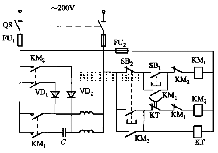
The circuit depicted in Figure 3-150 involves a contactor (KM1) that releases when the system is shut down. The contactor KM2 is energized, allowing a 220V AC power supply to flow through diodes VD1 and VD2, which serve as...
Warning: include(partials/cookie-banner.php): Failed to open stream: Permission denied in /var/www/html/nextgr/view-circuit.php on line 713
Warning: include(): Failed opening 'partials/cookie-banner.php' for inclusion (include_path='.:/usr/share/php') in /var/www/html/nextgr/view-circuit.php on line 713