
high power amplifier 300w circuit
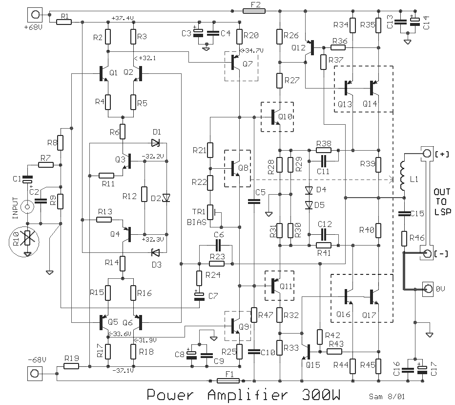
The described high-power amplifier circuit is engineered for robust performance in demanding audio applications. The input stage employs a complementary differential amplifier configuration, which enhances the linearity and gain of the signal. The use of low-power, high-gain transistors (Q1-Q9) ensures that the initial signal is amplified efficiently before being sent to the output stage.
The output stage is designed for substantial power amplification, allowing the amplifier to drive low-efficiency speakers and outdoor sound systems effectively. The configuration of Q10-Q11 and Q13-Q14 enables a significant power output while maintaining stability. The gain of this stage is carefully controlled by the resistors R44, R28, and R29, which ensures that the amplifier operates within its intended specifications.
Protection mechanisms integrated into the design, such as diodes D4 and D6, prevent potential damage from reverse biasing, while transistors Q12 and Q15 monitor the output conditions to safeguard against overcurrent and overvoltage situations. This attention to protective measures enhances the reliability of the amplifier in various operational environments.
Frequency response is crucial for audio fidelity, and the circuit incorporates multiple capacitors to define both the lower and upper frequency limits. The inclusion of thermal sensing via Q8 helps in maintaining optimal operating conditions, adjusting the bias current to accommodate variations in temperature.
Overall, this high-power amplifier circuit is meticulously designed to deliver exceptional performance, with features that enhance sound quality, protect components, and ensure longevity, making it suitable for a wide range of audio applications.There`s no substitute for sheer power- low efficiency speakers, outdoor sound systems, or maybe you like the full flavour of the dynamic range of a high power amp. Whatever your requirement-this super power module should fit the bill. How it works: The amplifier can be divided into three separate parts. These are : the input s tage, which consists of Q1-Q9, a high gain, low power driver; the output or power stage- witch only has a voltage gain of four but enormous power gain; and the power supply. The input stage is a complementary -differential network, each ``side`` with its own current source. Each transistor in this stage is run at a collector currant of about 0. 7mA. Emitter resistors are employed to stabilize the gain and improve linearity. The output of Q1-Q5 drives Q7 and Q9. The latter are virtually two constant-current sources run about 7mA collector current. With an input signal these ``current`` sources are modulated out of phase - the collector current of one decreases while the other increases.
This configuration provides quite an amount of gain. In between the bases of these two transistors is Q8, the thermal sensing-bias transistor. The voltage across Q8 may be adjusted by TR1, thus setting the quiescent bias current for output stage. The output stage, Q10-Q11, Q13-Q14 and Q16-17, has a gain of about five, set by R44 and R28 plus R29.
Diodes D4 and D6 prevent reverse biasing of Q10 and Q11 (otherwise the output would be limited). Protection of the output transistors is provided by Q12 and Q15 which monitor both current and voltage in the output transistors and bypass the base current if the limit is exceeded. Frequency stabilization provided by capacitors C6, C11, C12 and the RC networks R31/C10 plus R46/C15.
Frequency response of the amplifier is set by C1 and C7 (lower limit), C6 sets the upper frequency limit. If you want use the Protection DC and Balance/Bridge circuits. All the transistors that are inside the interrupted line are placed on an aluminium corner and he screwed on a suitable heatsink.
The transistors Q7, Q10, Q11, Q8, Q9, Q13, Q14, Q16 and Q17 placed on this aluminium corner, with suitable isolation from this. [ETI 4/80]. Download Part List 🔗 External reference
Related Circuits
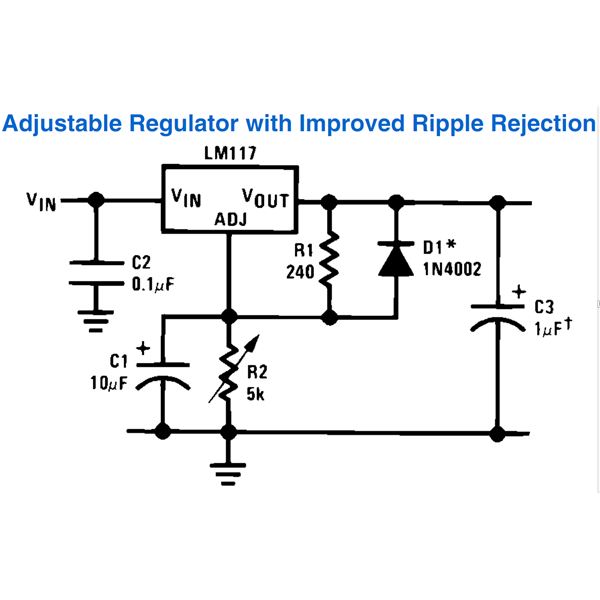
This document outlines the process of constructing an adjustable power supply utilizing the LM317 integrated circuit (IC). The LM317 is highly versatile, allowing for the creation of a wide variety of compact, high-quality power supply circuits. Various configurations can...
Using a Motorola MC2833 one-chip FM transmitter, a few support components, and an MPF6660 FET RF amplifier, this transmitter delivers approximately 3 W into a 50-ohm load. It is capable of operation over a frequency range of about 29...
This circuit is designed for use in a hi-fi showroom, allowing for the selection of different speakers to connect to a stereo amplifier for comparative listening. It can also serve similar applications where only one device from a set...
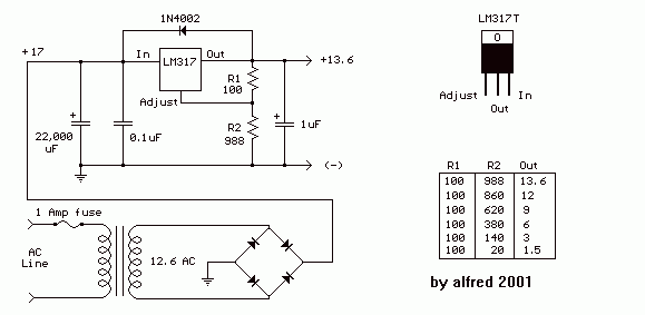
It's a variable power supply based on an LM317 voltage regulator. The range of power is between 1.6 and 13.5 volts, and it can provide up to 1.5 Amps if supplied with an adequate cooler, such as an aluminum...

The battery-operated black light utilizes a U-shaped, unfiltered black-light tube, which requires approximately 250 Vac for operation. To generate the 250 Vac from a 6-V battery, the circuit employs a one-transistor blocking oscillator that drives a ferrite inverter transformer....
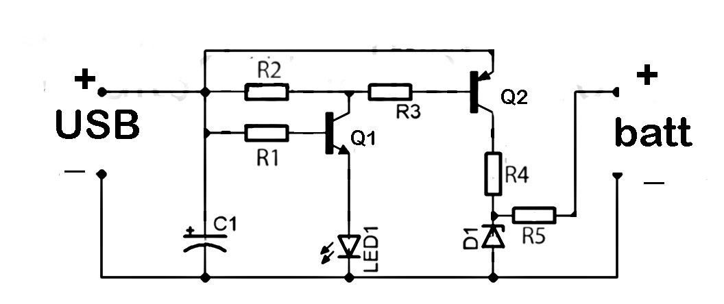
This document discusses the series used in USB connections for charging batteries. The output voltage ranges from 4.7 volts to 5 volts DC, which is suitable for charging mobile phones and other battery types. The circuit described enhances the...