
HIGH-SPEED DIGITAL DESIGN
The circuit design focuses on high-speed digital communication, emphasizing the importance of transmission line characteristics and impedance control to minimize signal integrity issues. The stacking of layers in the PCB is critical for optimizing the performance of the transmission lines, which must be carefully calculated to ensure that the characteristic impedance matches the requirements of the components used, particularly in high-speed applications. The moated ground area surrounding the crystal oscillator serves to isolate high-frequency noise, enhancing the stability of the oscillator and the overall circuit performance.
Pin/gate swapping is a technique employed to optimize the routing of signals on the PCB, facilitating a more efficient layout that can reduce trace lengths and improve signal integrity. The heat spreader design, utilizing vias to connect to the ground plane, aids in thermal management, ensuring that heat generated by the components is effectively dissipated, thereby maintaining operational reliability.
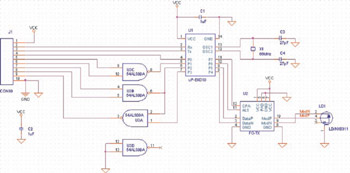
The microcontroller/digital signal processor (uP-EXD10) operates at a clock frequency of 66 MHz, making it suitable for applications requiring rapid data processing. The FO-TX interface IC enables the conversion of electrical signals to optical signals, facilitating communication over fiber optic cables. The inclusion of the fiber-optic laser diode (LD1) is essential for transmitting these optical signals, while the 54ALS00 NAND gates provide necessary logic functions for input/output operations, ensuring compatibility with various digital signal levels.
Overall, this example serves as a practical reference for designing high-speed digital PCBs, demonstrating key techniques and considerations for achieving optimal performance in modern electronic applications.This example demonstrates how to stack up layers and design transmission lines for a high-speed digital PCB. The example also demonstrates how to create a moated ground area with a bridge around a high-frequency crystal oscillator, how to perform pin/gate swapping, and how to create a heat spreader using vias to the Ground plane.
The example circu it is shown in Figure 9-156. The BOM for this example is shown in Table 9-8. The circuit consists of a (fictional) high-speed, low-pin-count microcontroller/digital signal processor (uP-EXD10) driven by a 66-MHz clock (X1), a digital to fiber optic interface IC (FO-TX, which mimics an ADN2530 but with fewer pins), a fiber-optic laser diode (LD1), and a couple of 54ALS00 NAND gates used for I/O decoding. The digital signals have rise and fall times from 200 ps to 1. 9 ns and require controlled impedance traces (see the Analog Devices ADN2530 data sheet for an example application).
In a real design, more bypass capacitors would be used on the circuit, but the design is scaled down to keep the design simple. The parts and footprints are located on the Web site for this book. 🔗 External reference
Related Circuits
Posts from PCB Schematic Design with DxDesigner tagged DxDesigner. The information pertains to the use of DxDesigner, a tool utilized for PCB schematic design. DxDesigner is part of the broader suite of design tools that facilitate the creation, editing, and...
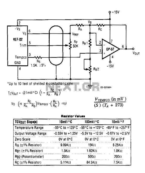
The DVM-to-temperature adapter is constructed around a single integrated circuit (IC), the National LM10. This micropower IC features a stable 0.2 V reference, a reference amplifier, and a general-purpose operational amplifier. The circuit is designed to operate within a...
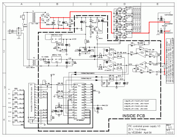
This is a variable power supply controlled by a PIC microcontroller. An LCD display is included in the circuit to show the actual output voltage and current values. A push-button switch is used to adjust the output voltage and...
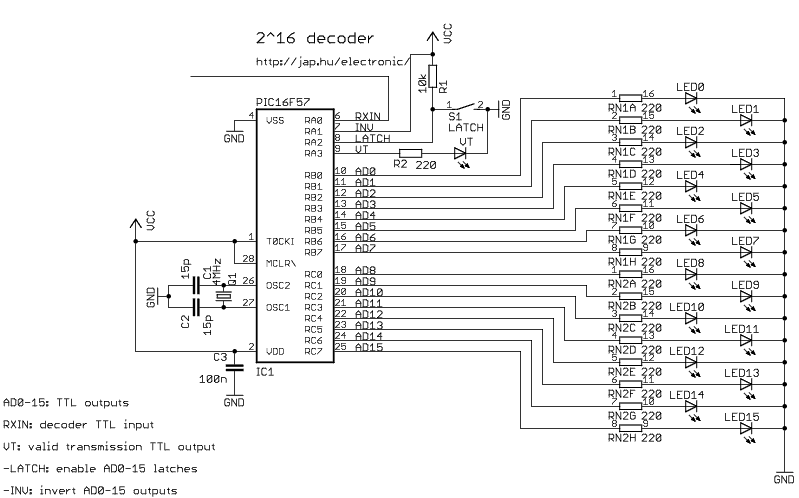
This encoder can transmit the state of up to 16 TTL digital inputs using an RF or infrared transmitter. When enabled, the included modulator automatically generates the 38kHz IR carrier. Containing a PIC microcontroller, the circuit is very flexible....
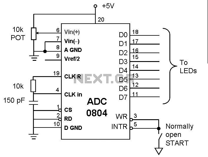
This post discusses the interfacing and operation of Analog-to-Digital Converters (ADCs). An ADC is a device that converts the analog signals from transducers into digital signals, enabling computers to process the data. ADCs are essential for obtaining meaningful results...
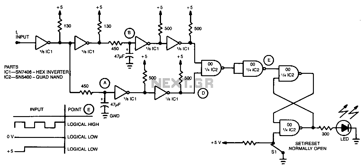
A simple inverter and NAND gate can be connected to create a highly compact and reliable digital frequency detector. This circuit is capable of detecting frequencies up to 3 MHz with a 50% duty cycle. When a frequency appears...