
analog to digital converter
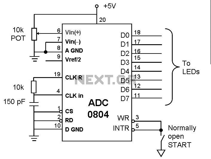
The ADC0804 chip features several important pins for operation. The RD (Read) pin is an active-low input used to retrieve converted data. When the chip select (CS) pin is low, applying a high-to-low pulse on the RD pin allows the 8-bit digital output to appear on the data pins D0-D7. The WR (Write) pin is another active-low input that initiates the conversion process. When CS is low and the WR pin transitions from low to high, the ADC0804 begins converting the analog input voltage (Vin) into an 8-bit digital number. Upon completion of the conversion, the INTR (Interrupt) pin goes low, signaling that the converted data is ready for retrieval. The clock input (CLK IN and CLK R) connects to an external resistor and capacitor for self-clocking, with the frequency determined by the formula f = 1/(1.1RC). The clock influences the conversion time, which cannot be faster than 110 microseconds. The INTR pin serves as an active-low output that indicates the end of the conversion process. After this signal, the CS pin is set low, and a high-to-low pulse is sent to the RD pin to access the converted data from the ADC0804.
The analog input pins Vin (+) and Vin (-) serve as differential inputs, where Vin is calculated as Vin (+) - Vin (-). Typically, the Vin (-) pin is connected to ground, while the Vin (+) pin is designated for the analog input signal that requires conversion. The Vref/2 pin is used for reference voltage input. If this pin is left unconnected, the ADC operates with an input voltage range of 0 to 5 volts. This input is optional and is utilized only when the input signal range needs to be defined.This post is about the ADC interfacing and working. Thus we can say that we need to have some means to convert the analog signal of transducers into digital signal so that computers can handle it and further processing could be done. Analog-to-digital converter (ADC) is a device which can convert analogue voltage to digital numbers so that microcontrollers can handle and process the data.
This is required to obtain some meaningful results or any useful work with micro controller. ADCs are the most widely used devices for data acquisition and control. Some microcontrollers have built in ADCs but the 8051 microcontroller don`t have any built in ADC. So we have to use external ADC for said purpose. There some common and important features about ADCs. for example, resolution of adc, response time of adc, mode of work and method of conversion. ADC has n-bit resolution, where n can be 8, 12, 16 or even 24 bits. The higher-resolution ADC provides a smaller step size. Step size is the smallest change that can be recognized by ADC. The heart of any current computational device relies upon digital bits, voltage states which can be at either high or low voltages. One of the simplest constructions, the ADC, converts an analog voltage signal to a digital one. Analog to Digital converters, and their counterparts, Digital to Analog converters are used all the time in electronics.
Indeed, they provide the only method by which one may interface a digital system with the real world, which functions in analog. Digital data acquisition and conversion systems are ubiquitous, being found in virtually every modern communication, digital signal processing (DSP), electronic instrument, and micro-controller applications.
Regardless of the sophistication of the application, a data acquisition and/or conversion system will consist of some pre-processing elements, a domain conversion device (digital to analog conversion (ADC) or analog to digital conversion (DAC), controller, and post-processing agent. RD (data enable) : Active low input used to get converted data out of the ADC0804 chip. When CS = 0, if a high-to-low pulse is applied to the RD pin, the 8-bit digital output shows up at the D0-D7 data pins.
WR (start conversion): Active low input used to inform the ADC0804 to start the conversion process. If CS = 0 when WR makes a low-to-high transition, the ADC0804 starts converting the analog input value of Vin to an 8-bit digital number. When the data conversion is complete, the INTR pin is forced low by the ADC0804. CLK IN and CLK R : Connect to external capacitor and resistor for self-clocking, f = 1/(1. 1RC). The clock affect the conversion time and this time cannot be faster than 110 micros. INTR (end of conversion) This is an active low output pin. When the conversion is finished, it goes low to signal the CPU that the converted data is ready to be picked up.
After INTR goes low, we make CS = 0 and send a high-to-low pulse to the RD pin to get the data out of the ADC0804 chip. Vin (+) and Vin (-) :These are the differential analog inputs where Vin = Vin (+)- Vin (-). Often the Vin (-) pin is connected to ground and the Vin (+) pin is used as the analog input to be converted to digital.
Vref/2 :- Input voltage pin used for the reference voltage. If this pin is open, the analog input voltage for the the ADC is ranged from 0 to 5 volts. This is optional input pin. It is used only when the input signal range 🔗 External reference
Related Circuits
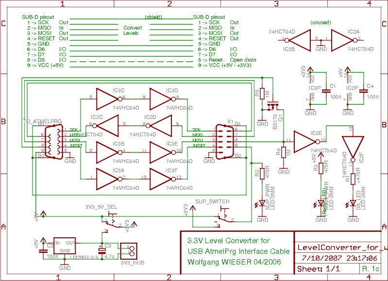
To program devices operating at 3.3V, such as SPI-based AVRs or JTAG-based CPLDs, level conversion is necessary for input and output signal levels. A 5V input may not register as HIGH at 3.3V, and a 3.3V device can be...
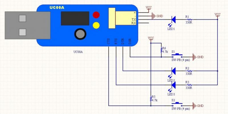
The LEDs operate in an active-low configuration (0), while the initial state of the switches is high (1). In other words, the PC software must send a low signal (0) to activate the LEDs, and if a low signal...
Free domains and hosting with up to 1GB of disk space, unlimited transfer, and access to PHP as well as 5 MySQL databases. The maximum size of a single file is not limited. This service offers a robust web hosting...
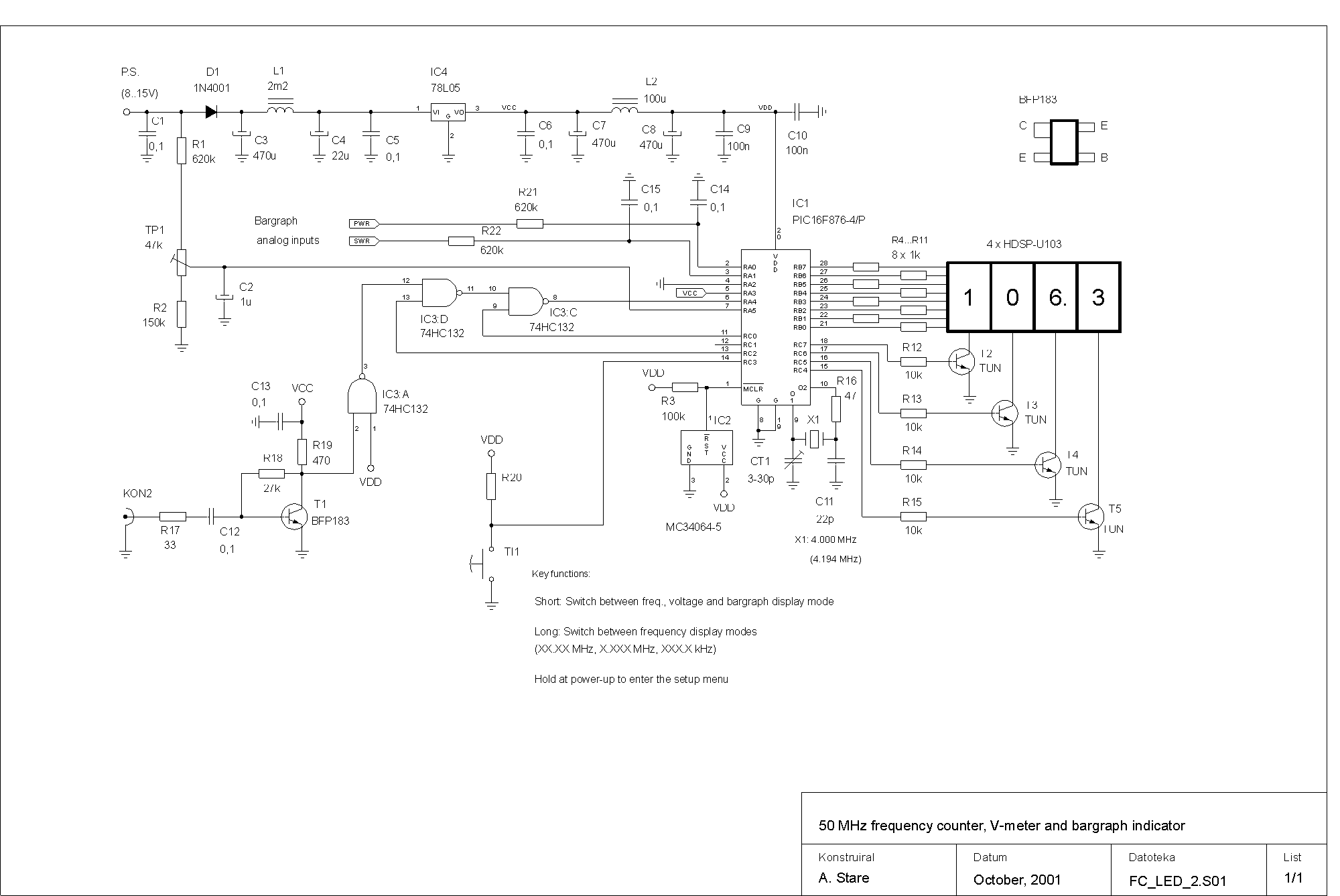
The frequency counter is designed to measure the number of cycles per second of an incoming signal. A counting device is necessary for this purpose, and in electronic circuits, counter integrated circuits (ICs) are available for counting input pulses....
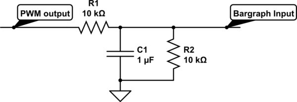
For a project, there is a need to display a progress bar representing the activity performed by a microcontroller unit (MCU). A bar graph display is intended for this purpose; however, the bar graph display driver IC, LM3914, requires...
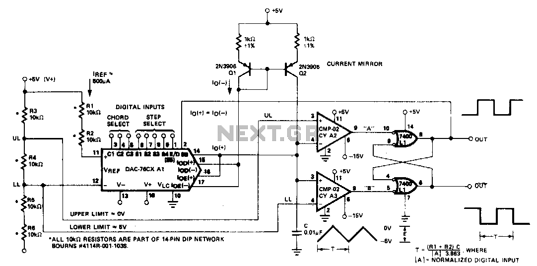
The microprocessor-controlled oscillator has a frequency range of 8159 to 1, covering from 2 Hz to 20 kHz. An exponential, current output integrated circuit digital-to-analog converter (DAC) functions as a programmable current source, alternately charging and discharging a capacitor...
Warning: include(partials/cookie-banner.php): Failed to open stream: Permission denied in /var/www/html/nextgr/view-circuit.php on line 713
Warning: include(): Failed opening 'partials/cookie-banner.php' for inclusion (include_path='.:/usr/share/php') in /var/www/html/nextgr/view-circuit.php on line 713