
How to design 65nm FPGA DDR2 memory
The article emphasizes the importance of "correctness by design" in DDR2 interfaces, particularly from a Signal Integrity perspective. This approach focuses on preemptively addressing potential design errors, which can significantly impact the performance of DDR2 memory systems. By analyzing common pitfalls encountered in DDR2 designs, engineers can make informed decisions regarding design alternatives that balance performance and reliability.
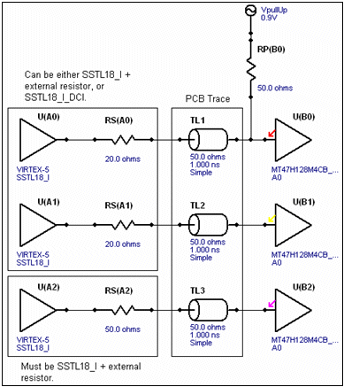
The schematic representations in the figures provide critical insights into effective design practices. The preferred usage model depicted in Figure 1 highlights the optimal configuration for DDR2 interfaces, ensuring that the memory chip operates as the driver and the FPGA as the receiver. This configuration allows for the effective use of the FPGA's DCI capabilities, which are essential for maintaining signal integrity across the bi-directional data lines.
Figures 1 and 2 not only illustrate the preferred topology but also showcase variations that are often employed in real-world design scenarios. Understanding these variations can help engineers avoid common mistakes and improve the robustness of their designs. The inclusion of input switching thresholds as dashed blue lines serves as a reference point, aiding in the evaluation of the receiver's performance under different conditions.
The use of Mentor Graphics' HyperLynx software to generate eye diagrams is a valuable tool for visualizing the signal integrity of the DDR2 interfaces. Eye diagrams provide a graphical representation of the signal quality and timing characteristics, allowing designers to assess the impact of their design choices on overall system performance. By utilizing eye diagrams generated with specific parameter settings, engineers can fine-tune their designs to achieve optimal signal integrity and reliability in DDR2 memory applications.This article presents practical techniques for incorporating "correctness by design" in DDR2 interfaces, from a Signal Integrity (SI) perspective, using the current generation of available design tools. Some common DDR2 design errors are analyzed, as well as the tradeoffs between some popular design alternatives.
Several possible address/control t opologies for DDR2 shown in Fig 1, while several possible data topologies are illustrated in Fig 2. In order to make use of the FPGA`s on-die digitally controlled impedance (DCI), the memory chip was made the driver and the 65nm FPGA device the receiver on the bi-directional data lines. The top schematic diagram in Fig 1 shows the preferred and recommended use model, while the other figures illustrate variations often attempted in regular design practice.
The input switching thresholds of the receiver are shown as horizontal dashed blue lines for reference. The color of the "probe" arrows in Fig 1 and Fig 2 correspond to the colors of the associated traces in Fig 3 and Fig 4, respectively.
Mentor Graphics` HyperLynx software was used to generate eye diagrams with the following parameter settings: 🔗 External reference
Related Circuits
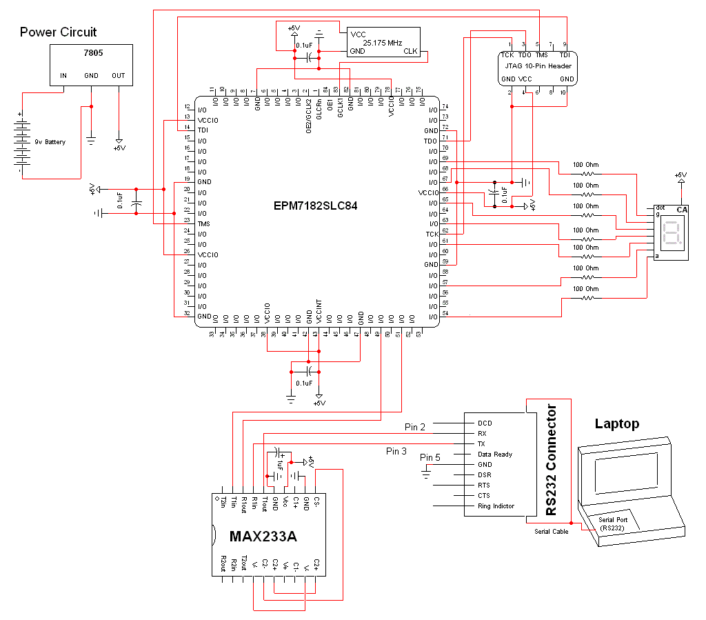
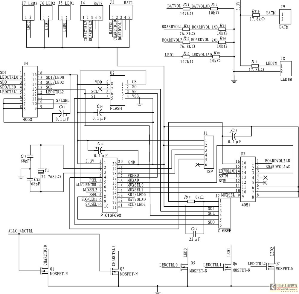
The schematic for this project is a modified version of the CPLD development board schematic. Several new components have been added for this project, and the completed schematic can be viewed below. The main components in the schematic are...
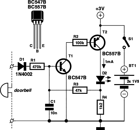
If you are expecting an important visitor but need to step out for a moment, an electronic doorbell memory can be useful to check whether someone rang while you were away. While it cannot confirm if it was the...
In daily life and production, many situations such as vehicle rollback, robot obstacle avoidance, industrial well logging, and liquid level measurement in reservoirs require non-contact automatic distance measurement. Ultrasonic waves refer to sound waves produced by machinery in an...
The development of a solar energy street lamp control device has progressed through three stages. The first generation featured a simple and crude function, allowing the light to be turned on or off, but required connection to a light-sensitive...
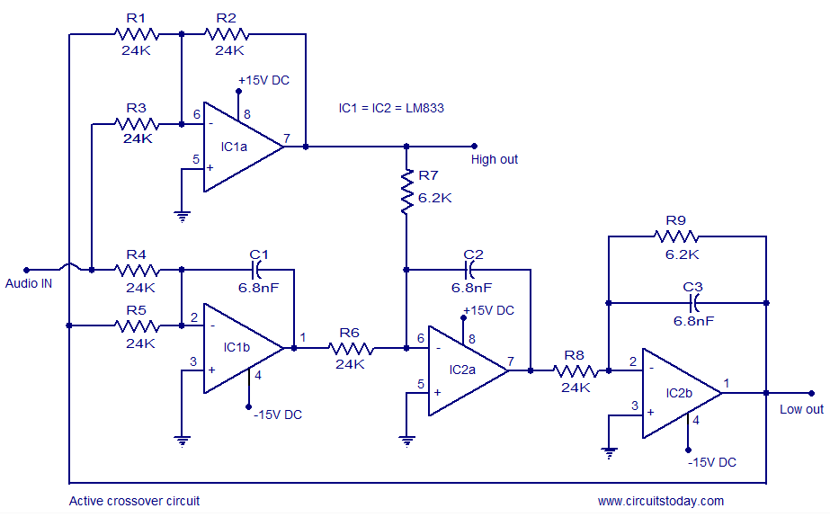
Active crossover circuit design, circuit diagram, schematic, DIY active crossover circuit, HiFi audio crossover, 2-way crossover circuit using LM833. The active crossover circuit is an essential component in high-fidelity audio systems, allowing for the separation of audio signals into different...
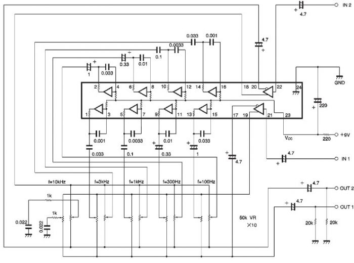
The BA3822 is a five-point stereo graphic equalizer integrated circuit that operates with two channels. Each channel can independently set five center frequencies using external capacitors. This integrated circuit supports a wide operating power supply voltage range (VCC =...