
FPGA RS232 Serial Interface Circuit
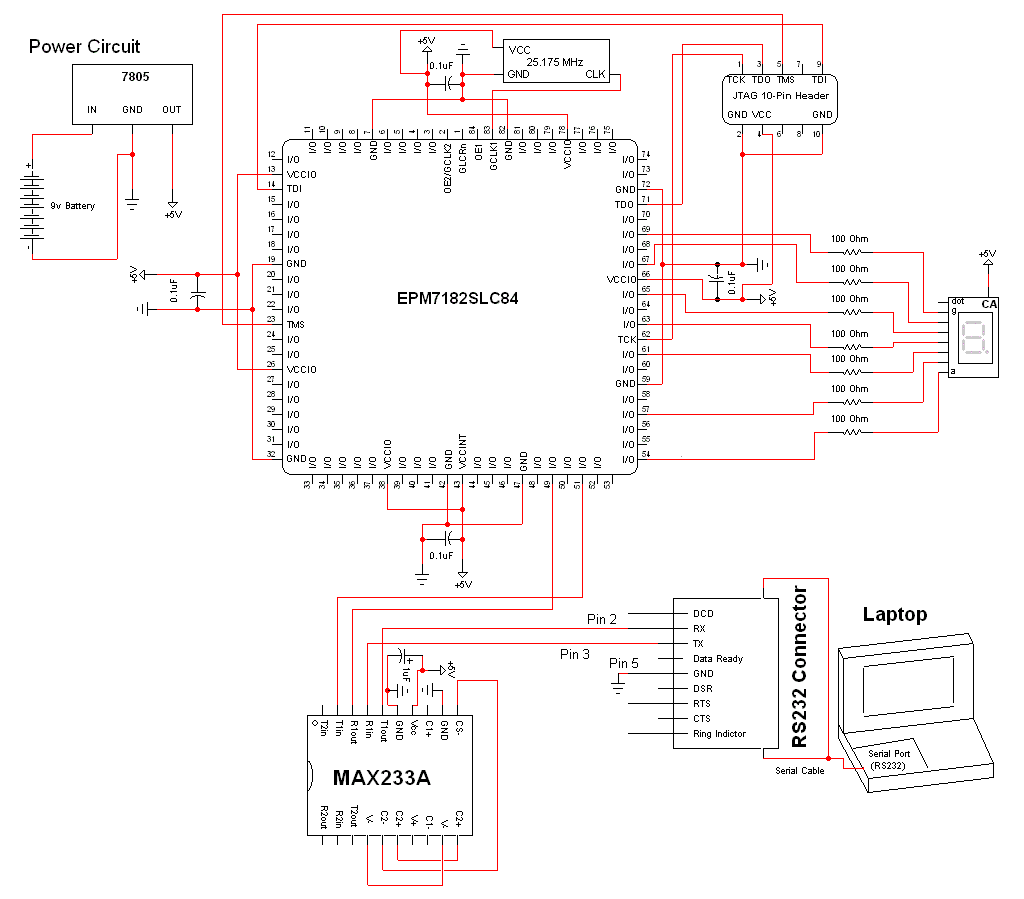
The project schematic integrates several key components to facilitate communication and processing. The CPLD (Complex Programmable Logic Device) serves as the core of the design, allowing for flexible logic configuration and control. The MAX233A is a critical component responsible for interfacing RS232 signals with the CPLD. It effectively translates the higher voltage levels of RS232 communication, which typically operate at ±12V, into TTL logic levels compatible with the CPLD's inputs and outputs. This translation is essential for ensuring reliable data transmission between the CPLD and any RS232 compliant devices.
The 5 MHz crystal oscillator provides the necessary clock signal for the CPLD, enabling synchronized operations within the circuit. This frequency is adequate for many applications, but higher frequencies can be utilized if required by the specific needs of the project. The selection of the oscillator was made based on availability, demonstrating the importance of having accessible components in the design process.
The 7-segment display is utilized in this schematic to provide a visual output, allowing users to observe the results of the CPLD's processing. The display is driven by the CPLD, which controls each segment's illumination based on the logic implemented in the device. This feature enhances the usability of the project by providing immediate feedback on its operation.
Overall, the modified CPLD development board schematic represents a practical implementation of digital logic design, showcasing the integration of various components to achieve a functional prototype. The choice of parts and their arrangement within the schematic reflects a balance between performance, availability, and ease of use, making this project a valuable reference for similar applications in electronics design.The schematic for this project is a modified version of the CPLD dev board schematic. There are a few new parts added for this project and you can see the completed schematic for this project below. The main parts in the schematic are the CPLD Dev Board, MAX233a and 7 Segment Display. The RS232 interface circuit consists of the CPLD, it`s 25. 17 5 MHz crystal clock and the MAX233A. The MAX233A translates the +12v higher voltage RS232 signals into TTL +5v logic that the FPGA can understand. This protoboard for a cpld was developed by me a few years ago. It`s really just a PLCC CPLD in a socket with power and JTAG connectors for programming. This oscillator was chosen mostly at random. We needed some type of timing device to keep a reference to time and I had this one laying around. Generally if you can find a clock above 10 MHz you`ll be fine for this project. 🔗 External reference
Related Circuits
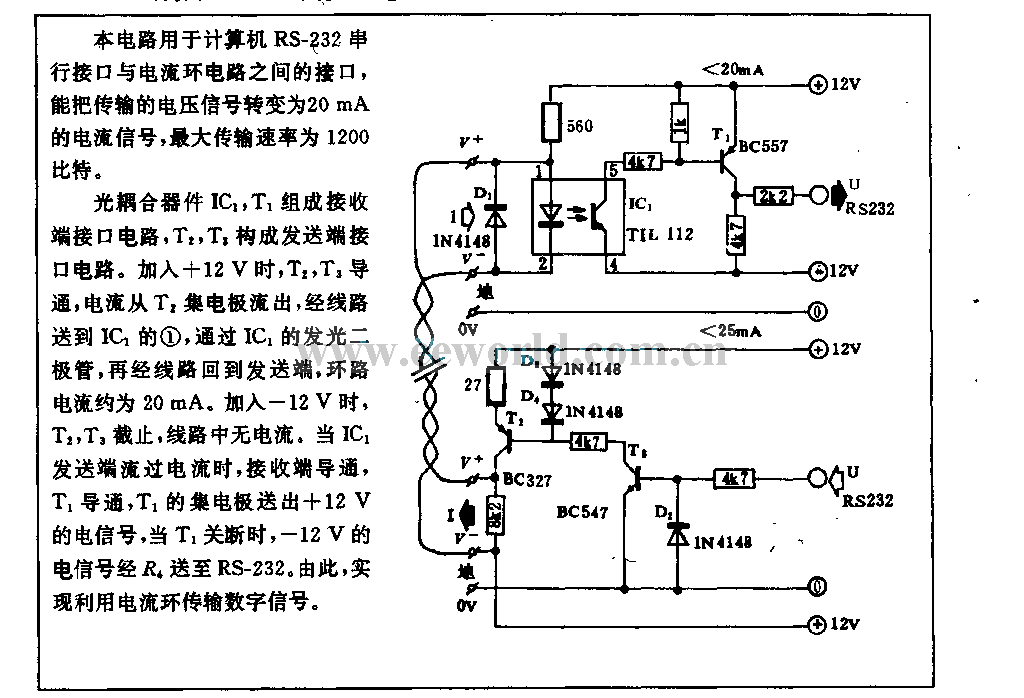
This circuit is utilized in RS-232 serial interface and current loop circuit applications. It converts voltage signals into a 20mA current signal, with a maximum transmission rate of 1200 bits per second. The CCD IC1 and transistor T1 form...
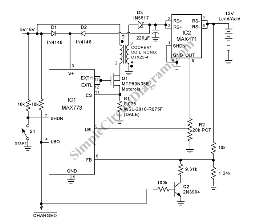
To charge lead-acid batteries, a circuit can be utilized that consists of a current-limited power supply and a flyback converter topology. The circuit designed for charging lead-acid batteries incorporates a current-limited power supply alongside a flyback converter topology to...
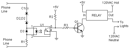
The inquiry pertains to the connection of lights that flash when a phone rings. This feature is particularly beneficial in noisy environments, such as workshops, where hearing the phone may be difficult. A device designed for this purpose is...
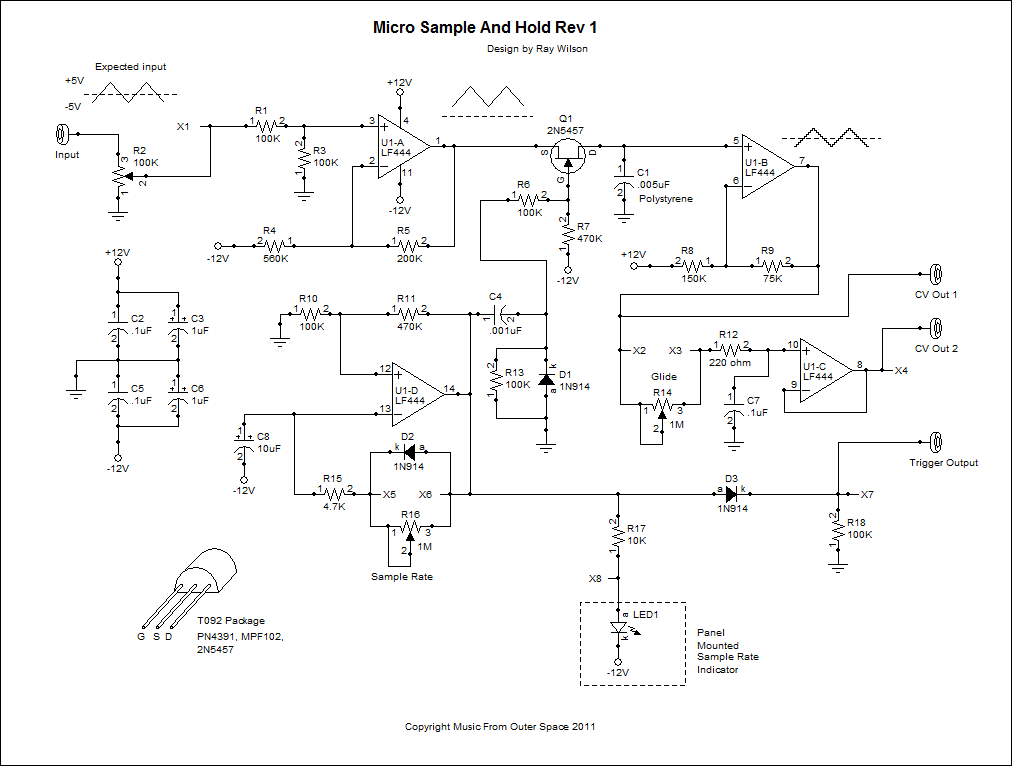
The voltage to be sampled is applied to the input of R2, a 100K linear taper potentiometer, while the other end of R2 is grounded. Consequently, the signal level that is sent to the buffering level shifter U1-A and...
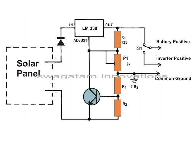
Solar panels are well-known devices that convert solar energy or sunlight into electricity. A solar panel consists of discrete sections of individual photovoltaic cells, each capable of generating a small amount of electrical power, typically between 1.5 to 3...
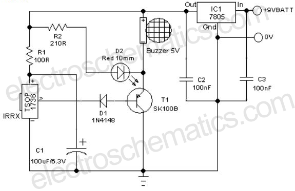
A remote-controlled alarm circuit utilizing the TSOP1736 is designed for easy use by elderly individuals or patients confined to bed. This battery-operated alarm system eliminates the need for routing electric cables to a calling bell switch, making it a...
Warning: include(partials/cookie-banner.php): Failed to open stream: Permission denied in /var/www/html/nextgr/view-circuit.php on line 713
Warning: include(): Failed opening 'partials/cookie-banner.php' for inclusion (include_path='.:/usr/share/php') in /var/www/html/nextgr/view-circuit.php on line 713