
HV REGULATOR WITH FOLDBACK CURRENT LIMIT

The circuit employs a current sensing mechanism through resistor R8, which allows for the monitoring of output current levels. This sensed current is then fed into a current-limit amplifier via resistor R7. The amplifier operates based on a foldback potential established by resistor R6, with the threshold for this operation being set by diode D4. The design ensures that the peak power output is limited to below 20 W, providing a safeguard against excessive power levels. If the voltage across the pass transistors exceeds 310 V, a protective mechanism is triggered to shut them off, thereby preventing damage to the circuit.
In scenarios where the unregulated input voltage surpasses 310 V, the circuit initiates a start-up sequence driven solely by the current flowing through resistor R5. The inclusion of transistor Q4 is critical, as it offers preliminary control over the current flow before the operational amplifier A2 can respond effectively. This feature enhances the responsiveness of the circuit during the start-up phase.
Stability of the circuit is maintained with the use of an output capacitor that exceeds approximately 2 F. This large capacitance helps to smoothen the output and mitigate any potential fluctuations. Additionally, to combat spurious oscillations that may arise during current limiting, capacitors C2 and resistor R4 are strategically placed to filter these disturbances. Furthermore, to address and eliminate any latch-mode oscillations that may occur as a result of current limiting, capacitors C1 and resistor R1 are employed. This comprehensive design facilitates reliable performance while safeguarding against various operational anomalies.The output current issensed across R8, This is delivered to the current-limit arrtplifier through R7, across which the foldback potential is developed by R6 with a threshold determined by D4. The values given limit the peak power below 20 W and shut off the pass transistors when the voltage across them exceeds 310 V.
With unregulated input voltage s above this value, start-up is initiated solely by the current through R5. Q4 is added to provide some control on current before A2 has time to react. The circuit is stable with an output capacitor greater than about 2 F. Spurious oscillations in current limit are suppressed by C2 and R4, while a strange, latch-mode oscillation coming out of current limit is killed with C1 and R1. 🔗 External reference
Related Circuits
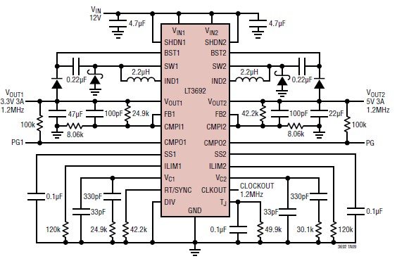
The LT3692 dual current mode PWM step-down DC-DC converter circuit, featuring two internal 3.5A switches, can be utilized to design a straightforward power supply circuit suitable for various electronic applications, including distributed supply regulations and automotive circuits. The LT3692...
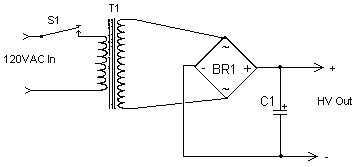
The circuit can produce about 250-500mA at 2KV, depending on the transformer. For C1, you can use the capacitor out of an old microwave. This circuit is mainly provided as a demonstration of using commonly available parts for something...
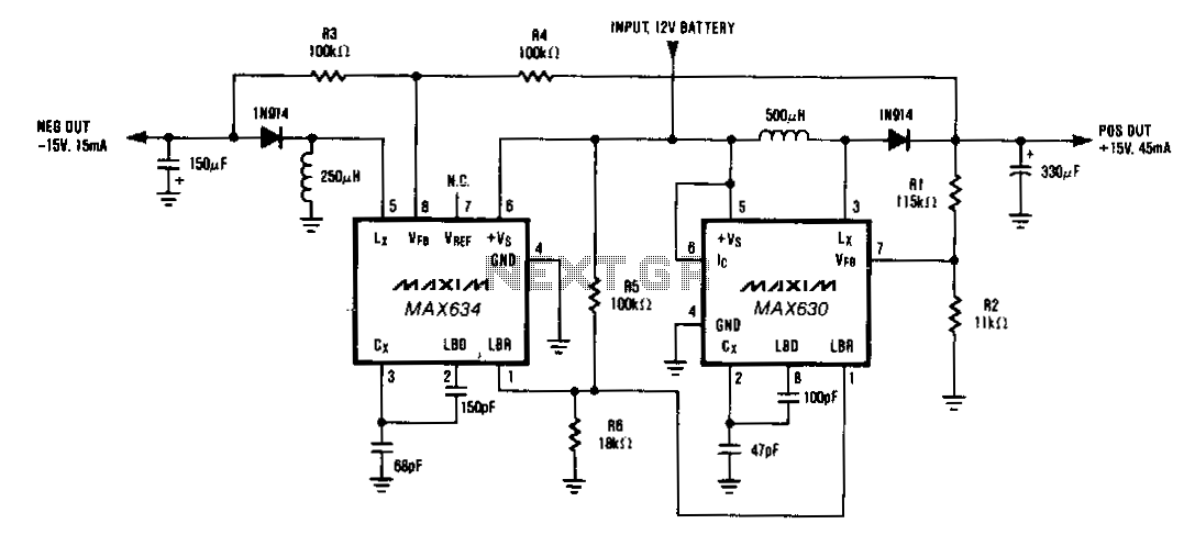
A MAX634 inverting regulator is combined with a MAX630 to provide a dual tracking ±15 V output from a 12-V battery. The reference for the -15 V output is derived from the positive output via resistors R3 and R4....
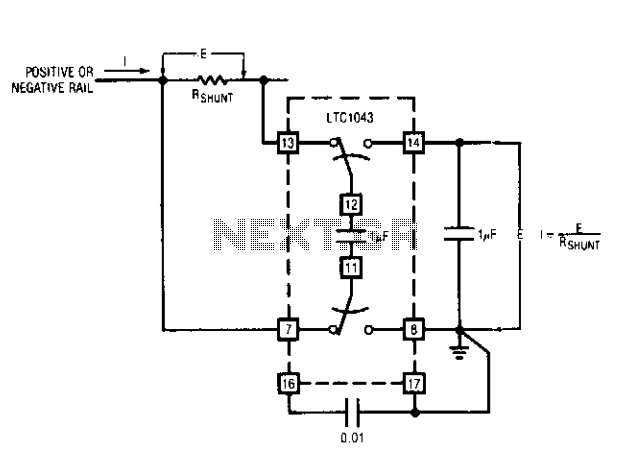
This capability has wide application in battery and solar-powered systems. If the ground-referred voltage output is unloaded by an amplifier, the shunt can operate with very little voltage drop across it, minimizing losses. The LTC1043 can sense current through...

This circuit allows for the establishment of a maximum output current limit from a power supply unit (PSU). It is particularly beneficial when initially powering a project or conducting a soak test. By imposing an upper current limit, protection...
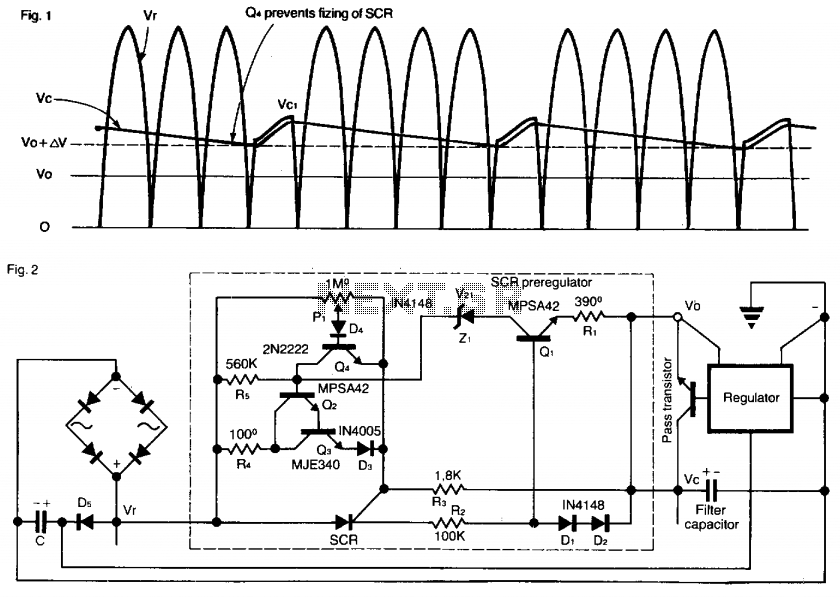
This SCR pre-regulator maintains the filter capacitor voltage (Vc) in a variable output power supply at a few volts above the output voltage (V0). The advantages include reduced heat dissipation by the pass transistor, resulting in a smaller heatsink,...