
Hybrid Headphone Amplifier
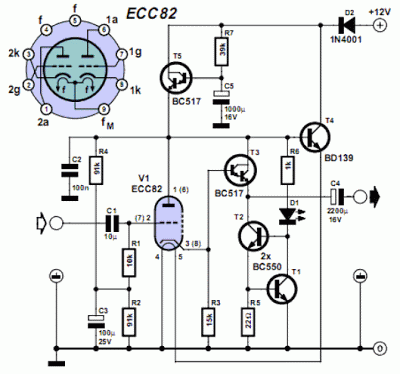
ther non-linear distortions. This design of a dedicated headphones amplifier is potentially controversial in that it has unity voltage gain and employs valves and transistors in the same design. Normal headphones have an impedance of 32R per channel. The usual standard line output of 775 mV to which all quality equipment aspires will generate a power of U2 / R = 0.
7752 / 32 = 18 mW per channel across a headphone of this impedance. An examination of available headphones at well known high street emporiums revealed that the sensitivity varied from 96 dB to 103db/mW! So, in practice the circuit will only require unity gain to reach deafening levels. As a unity gain design is required it is quite possible to employ a low distortion output stage. The obvious choice is an emitter follower. This has nearly unity gain combined with a large amount of local feedback. Unfortunately the output impedance of an emitter follower is dependent upon the source impedance. With a volume control, or even with different signal sources this will vary and could produce small but audible changes in sound quality.
This device, as opposed to a transistor configuration, enables the output stage to be driven with a constant value, low impedance. In other words, the signal from the low impedance point is used to drive the high impedance of the output stage, a situation which promotes low overall THD.
At the modest output powers required of the circuit, the only sensible choice is a Class A circuit. In this case the much vaunted single-ended output stage is employed and that comprises of T3 and constant current source T1-T2. The constant current is set by the Vbe voltage of T1 applied across R5 With its value of 22R, the current is set at 27 mA.
T3 is used in the emitter follower mode with high input impedance and low output impedance. Indeed the main problem of using a valve at low voltages is that it`s fairly difficult to get any real current drain. In order to prevent distortion the output stage shouldn`t be allowed to load the valve. This is down to the choice of output device. A BC517 is used for T3 because of its high current gain, 30, 000 at 2 mA! Since we have a low impedance output stage, the load may be capacitively coupled via C4. Some purists may baulk at the idea of using an electrolytic for this job but he fact remains that distortion generated by capacitive coupling is at least two orders of magnitude lower than transformer coupling.
The rest of the circuitry is used to condition the various voltages used by the circuit. In order to obtain a linear output the valve grid needs to be biased at half the supply voltage. This is the function of the voltage divider R4 and R2. Input signals are coupled into the circuit via C1 and R1. R1, connected between the voltage divider and V1`s grid defines the input impedance of the circuit. C1 has sufficiently large a value to ensure response down to 2 Hz. Although the circuit does a good job of rejecting line noise on its own due to the high impedance of V1`s anode and T3`s collector current, it needs a little help to obtain a silent background in the absence of signal. The help` is in the form of the capacitance multiplier circuit built around T5. Another BC517 is used here to avoid loading of the filter comprising R7 and C5. In principle the capacitance of C5 is multiplied by the gain of T5. In practice the smooth dc applied to T5`s base appears at low impedance at its emitter. An important added advantage is that the supply voltage is applied slowly on powering up. This is of course due to the time 🔗 External reference
Related Circuits
This circuit is primarily designed to provide a microphone input for standard home stereo amplifiers. Utilizing a battery supply minimizes the risk of low-frequency hum interference from mains power, simplifying the connection to the amplifier by eliminating the need...
300W Subwoofer Power Amplifier. High power amplifiers are not common as projects, as they are inherently challenging to build and often expensive. A minor error during assembly can lead to significant issues. The 300W subwoofer power amplifier is designed to...
Figure (a) illustrates a general inverting amplifier circuit, which includes a 100k potentiometer as a feedback resistor connected in series between the input terminal and the inverting input to compensate for the DC bias current. The potentiometer (Rp) should...
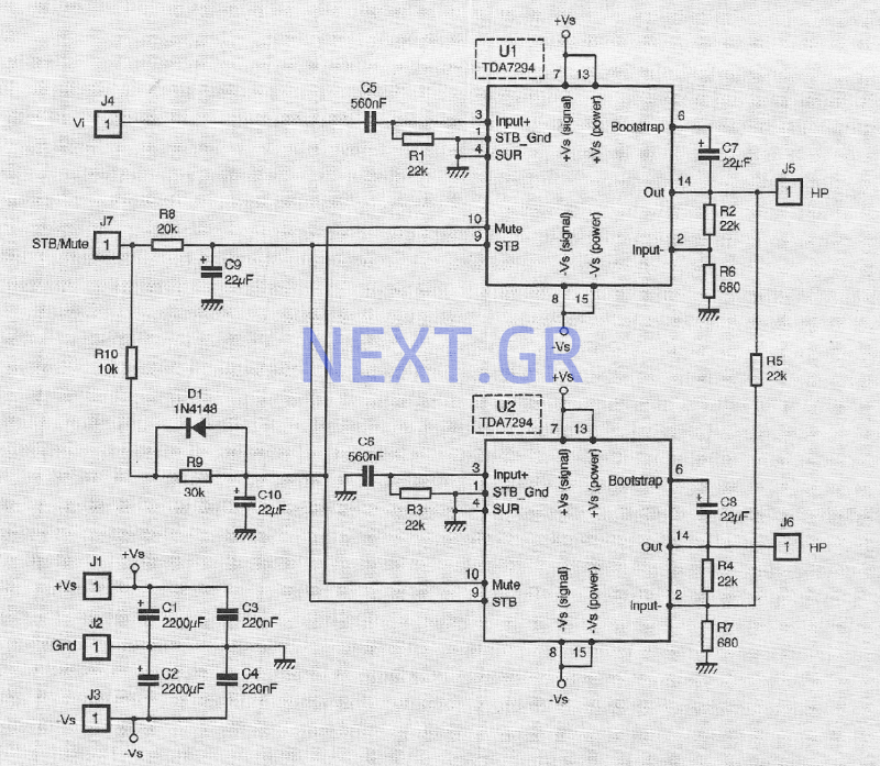
The TDA 7294 from T-MICROELECTRONICS is a monolithic integrated circuit housed in a "Multiwatt 15" package, primarily designed for use in Class AB amplifiers for high-fidelity applications, including stereo systems, active speakers, and television receivers. Its large feed area...
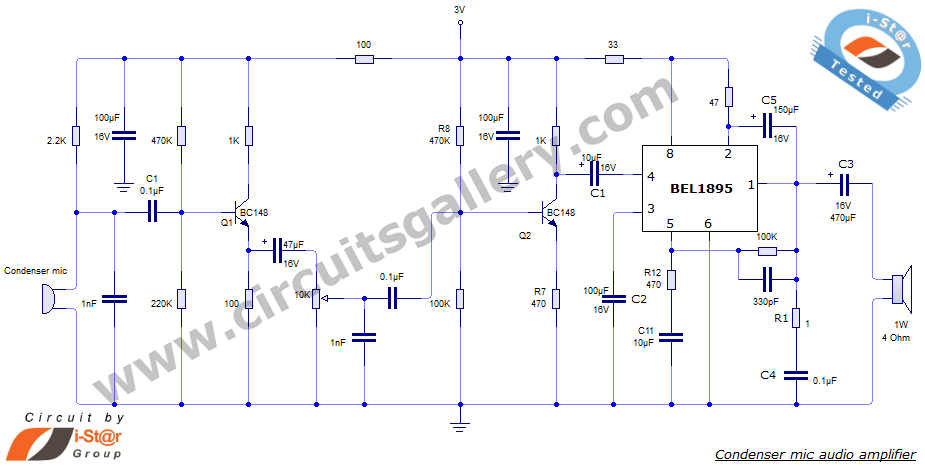
This document presents an audio amplifier circuit suitable for use in walkie-talkies, low-power transmitters, and packet radio receivers. The circuit utilizes a condenser microphone audio amplifier that delivers high-quality audio output of 0.5 watts at 3 volts. The design...
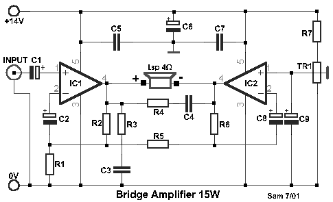
This is a compact collection of amplifiers configured in a bridge connection. The output power is low, making them suitable for general applications. They can be utilized with small active loudspeakers, car stereos, and similar devices. The only limitation...