
Broadband amplifier with bias compensation circuit diagram
The inverting amplifier circuit described is a fundamental building block in analog signal processing, functioning to invert and amplify input signals. The inclusion of the 100k potentiometer as a feedback resistor allows for fine-tuning of the circuit's gain, providing flexibility in applications requiring precise control over output levels. By setting the potentiometer to achieve a zero output voltage when the input is also zero, the circuit maintains stability and accuracy in signal processing.
The phase compensation capacitor (C1) plays a crucial role in stabilizing the amplifier by managing the phase shift introduced by the feedback network. This is particularly important in high-frequency applications where phase shifts can lead to instability and oscillation. The additional filter capacitor (C2) aids in reducing noise and improving the overall signal integrity.
With a voltage gain of -10, the circuit can effectively amplify signals while inverting their polarity. The specified slew rate of over 70V/s indicates the circuit's ability to respond rapidly to changes in input signals, making it suitable for dynamic signal applications. The bandwidth of over 400kHz ensures that the amplifier can process a wide range of frequencies, making it versatile for various electronic applications.
The gain-bandwidth product of approximately 30MHz suggests that as the gain increases, the bandwidth decreases, adhering to the principles of operational amplifier behavior. This characteristic is essential for designers to consider when selecting the amplifier for specific applications, ensuring that the desired gain does not compromise the frequency response.
The LH0003 integrated circuit is housed in a 10-pin circular metal package, which provides durability and thermal stability. The specified operating temperature ranges ensure reliable performance in diverse environmental conditions, making it suitable for industrial and commercial applications. The pin configuration detailed in Figure (b) facilitates easy integration into larger circuit designs, allowing engineers to leverage the capabilities of the LH0003/LH0003C in their electronic systems.Figure (a) shows the circuit with general inverting amplifier circuit differs only in that series with a 100k potentiometer feedback resistor between the input terminal and the inverting input, to compensate for the DC bias current. Adjust the potentiometer Rp, so when Vi 0V when, Vo 0. Indirect compensation pins for phase compensation capacitor C1 (90pF) 1 and 10, the pin 5 to ground filter capacitor C2 is also 90pF. The circuit shown in the voltage parameters of magnification: Av -10, its speed is greater than the voltage converter 70v/s, more than half-power bandwidth of up to 400kHz, the gain-bandwidth product of approximately 30MHz.
10-pin package LH0003 circular metal operating temperature is 0 ~ 85, storage temperature is -65 ~ 150. When LH0003 chip, the operating temperature of -55 ~ 125, storage temperature is -65 ~ 150. Figure (b) is LH0003/LH0003C integrated chip pin arrangement of FIG.
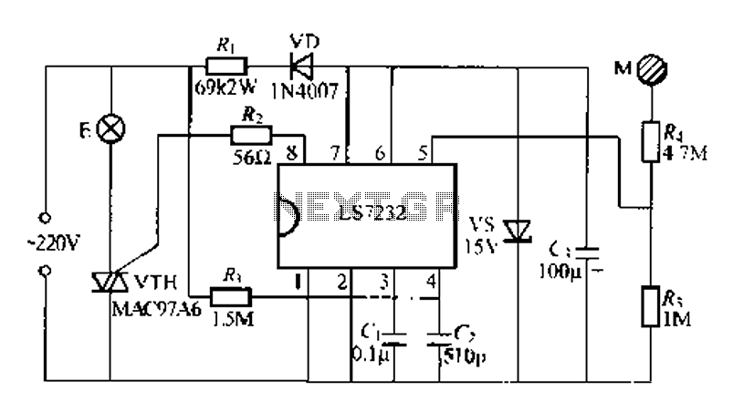
Related Circuits
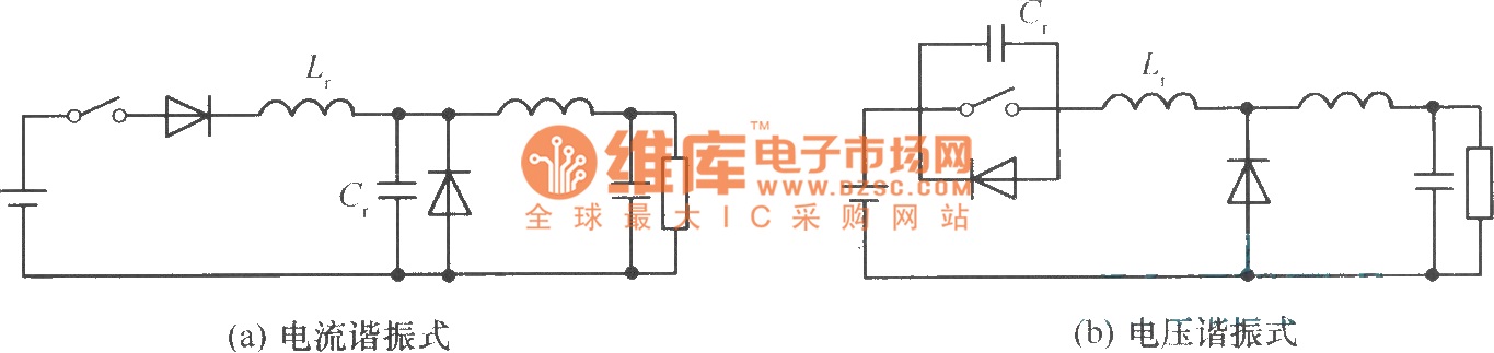
In a commonly used switching stabilized voltage supply, a resonant switch can be utilized to replace the shape of a step-down converter, resulting in a resonant converter circuit. The diagram illustrates the transformation from a step-down converter to a...
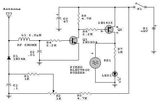
This electronic RF detector project is constructed using common transistors and a few standard electronic components. The RF detector is capable of responding to RF signals below the standard broadcast band and extending to over 500 MHz, providing both...
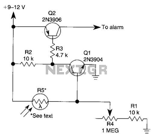
The circuit functions as a sensor capable of triggering an alarm without direct contact from an intruder. It utilizes a visible or invisible light source that illuminates the sensor, maintaining the detection loop in a normally closed state. As...
This design circuit project involves a clear glass sensor circuit intended for experimental or hobbyist applications. The concept is straightforward and relies on a homemade sensor unit that includes one high-efficiency ultra-bright red LED (D1) and a standard phototransistor. The...
After integrating the negative feedback circuit, the adjustment object and inertial measurement feedback link are susceptible to oscillations. To address this, a voltage differential or speed differential circuit is employed to minimize or eliminate these oscillations, serving as a...
A simple synthesized 13 cm ATV exciter has led to considerations for an appropriate power amplifier. The exciter generates approximately 10 mW, which may be sufficient to drive a MMIC or hybrid amplifier. However, at 2.3 GHz and higher...