
IB31 internal functional block diagram and pin functions

The Analog Devices 1831 integrated circuit (IC) is specifically engineered for the precise conditioning of signals from strain gauges. Its internal architecture includes a low drift input voltage of 0.25V, which is amplified by a gain factor of 1000, ensuring that even the smallest variations in strain are accurately captured and processed. The device's remarkable linearity, with a maximum deviation of only 0.005%, facilitates high-fidelity signal reproduction, making it suitable for applications requiring stringent accuracy.
Noise performance is critical in strain gauge applications, and the 1831 excels in this aspect with a noise level of merely 0.3 pVp-p at a frequency of 0.1 Hz, ensuring that the output signal remains clean and reliable. Additionally, the high common-mode rejection ratio (CMRR) of 140 dB at 60 Hz indicates the device's ability to effectively eliminate common-mode signals, further enhancing the integrity of the output.
The instrumentation amplifier within the 1831 is capable of driving resistive loads of 120 ohms or higher, making it versatile for various configurations of strain gauge circuits. The inclusion of a negative charge pump circuit allows the IC to provide a stable output of +4V from a +15V supply, which can be advantageous for powering other components in the system.
Moreover, the device features a reference voltage source circuit that aids in maintaining consistent output levels. The output drift is impressively low at 0.004%, which is essential for long-term stability in precision measurements. The output offset voltage can be fine-tuned using an external resistor, allowing for adjustments over a range of 10V, which is beneficial for calibrating the system to meet specific requirements.
The operating supply voltage range of the 1831 is between 12V and 18V, providing flexibility in integration with various power supply configurations. The detailed pin functions and internal functional block diagram provide a comprehensive overview of the IC's capabilities, assisting engineers in effectively implementing the device in their designs. Overall, the Analog Devices 1831 is a robust solution for strain gauge signal conditioning, delivering high performance and reliability in demanding applications.Analog Devices 1831 to produce strain gauge signal conditioning ICs, contains an internal low drift input 0. 25V, V/qC (RTI, G 1000), excellent linearity (maximum 0.005%), low noise (0.3pVp. P, O.1. 10Hz), high CMRR (140dB, C 1000,60Hz) instrumentation amplifier can drive resistive 120fl greater than the negative charge pump circuit bridge (+4 output a + 15V), a reference voltage source circuit, etc.. Output drift only 0.o04% Gate C, the output offset voltage can be adjusted by an external resistor range of 10V.
Operating supply voltage range of (12-18) V. 1831 pin functions and internal functional block diagram shown in Figure
Related Circuits
The 5 V from USB appears to be powering the LED on the laptop power brick. Therefore, even when the power brick is turned off at the wall outlet, the LED remains illuminated. When the USB is unplugged, the...
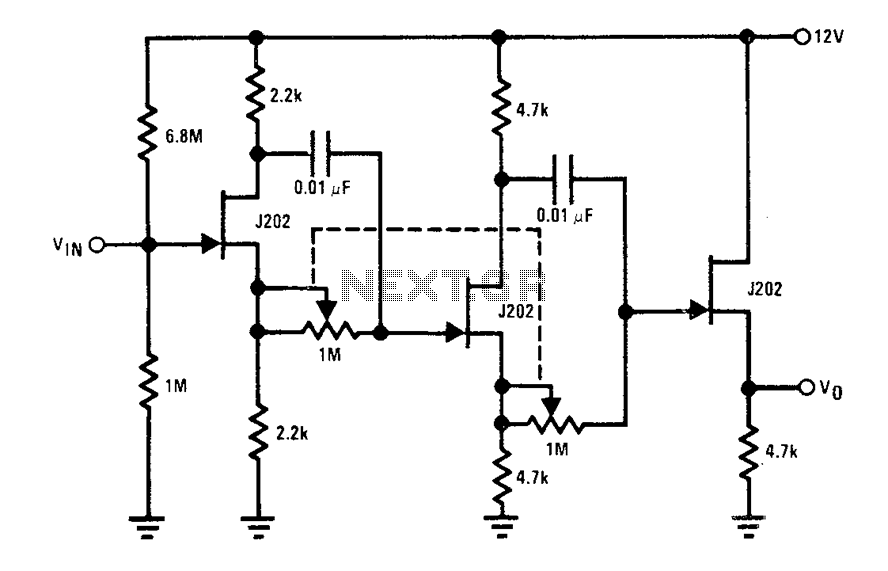
Each J202 JFET stage provides up to 180 degrees of phase shift controlled by a 1 megohm potentiometer. The potentiometer allows for complete control of the groups. JFETs are ideal for the designated circuit because they do not load...

The circuit features a dual-core 556 timer IC and a light-emitting diode (LED) tube. The left half of the IC (556 1/2) comprises resistors R1, R2, capacitor C1, etc., generating a frequency of approximately 2 Hz in a multivibrator...
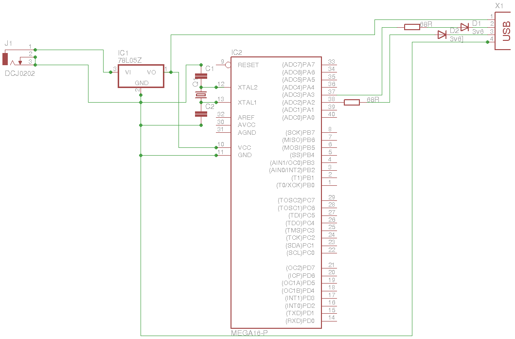
Development board for 18-pin PIC microcontrollers featuring a power supply circuit, crystal oscillator circuit, RS232 port, ICSP/ICD port, 4 relay outputs, and 4 optocoupler isolated inputs. This development board is designed to facilitate the prototyping and testing of applications utilizing 18-pin...
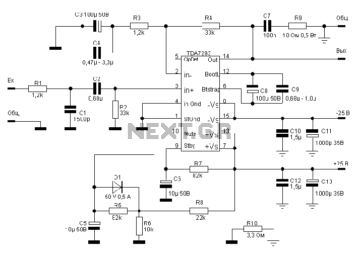
The TDA7293, produced by the ST (SGS-THOMSON) company, is a high-power, high-voltage DMOS high-fidelity amplifier integrated circuit (IC) with a rated output power of 100W. It operates at a maximum voltage of 120V. The key specifications include a dual...
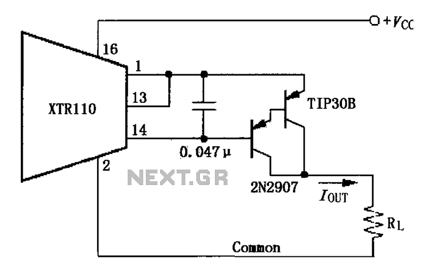
The circuit consists of two discrete PNP Darlington transistors that form the external PNP transistor QEXT circuit to enhance output current. The use of integrated Darlington transistors is not recommended, as the internal base-emitter resistor can introduce additional errors....