
IDE interface project
The IDE interface board facilitates communication between a hard drive and the host computer, utilizing the Integrated Drive Electronics (IDE) standard. This board typically includes a connector for the hard drive, a power supply interface, and necessary components to manage data transfer. The use of the AMD PALCE16V8Q-15 decoder chip allows for custom logic implementation, which enhances the interface's capability to manage various data protocols and control signals effectively.
The driver software is essential for enabling the operating system to interact with the hardware. It translates high-level commands from the OS into low-level instructions that the IDE interface can understand. The development of this driver involves not only coding but also extensive testing to ensure reliability and performance under the OS-X 2.0 Real-Time Operating System (RTOS). The experimental driver provided in the accompanying zip file serves as a foundational example, showcasing the essential functions required to read from and write to the hard drive.
The provided schematic and PCB layout files are crucial for understanding the electrical connections and component placements on the IDE interface board. These documents are instrumental for engineers looking to replicate or modify the design. Additionally, the inclusion of PALASM source code and JEDEC files allows for further customization of the logic functions implemented within the PAL device, enabling users to adapt the interface to specific requirements or to troubleshoot issues that may arise during operation.
Overall, the combination of hardware and software resources outlined serves as a comprehensive starting point for developing a fully functional IDE interface for use with the OS-X 2.0 RTOS on the Z180 architecture.An IDE interface board and I`m currently working on the driver software to support reading/writing on a hard drive under my OS-X 2. 0 RTOS. An assembled IDE interface board is shown below. Download pcb. zip which contains the schematic and PCB layout files in Adobe Acrobat (. pdf) format. It also contains PALASM source and JEDEC file for the AMD PALCE16V8Q-15 decoder chip used. Download driver. zip which contains source code for my experimental driver and test program. The program runs on OS-X 2. 0 on my Z180 computer. Please note that this is NOT the final driver program. There are a number of optimizations left to implement. It should be regarded as an example of how to use my IDE interface. 🔗 External reference
Related Circuits
Voltage inverter circuit design electronic project using few electronic components The voltage inverter circuit is a fundamental electronic project that converts direct current (DC) to alternating current (AC). This circuit is particularly useful in applications where AC voltage is required...
The task involved implementing and programming all hardware devices to make data accessible to the receiver program running on a PC. This included configuring all Prospeckz devices and establishing protocols for radio transmission communication back to the PC. Additionally,...

The A/B switch circuit comprises three integrated circuits (ICs) and several resistors. Two gates from a 4011 quad 2-input NAND gate (U1A and U1B) are configured as a monostable multivibrator. When switch SI is activated, it triggers a 4017...
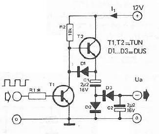
The logic input is applied to opto-isolators U1 and U2, which utilize npn and pnp emitter follower outputs, respectively. DC balance is adjusted using potentiometer R2. The emitter followers drive the gates of Q1 and Q2, which are complementary...
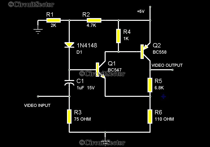
There are instances when it is necessary to view video clips captured by a digital camera on a television. This can be accomplished by connecting the camera's video output to the television's video input. However, a direct connection is...
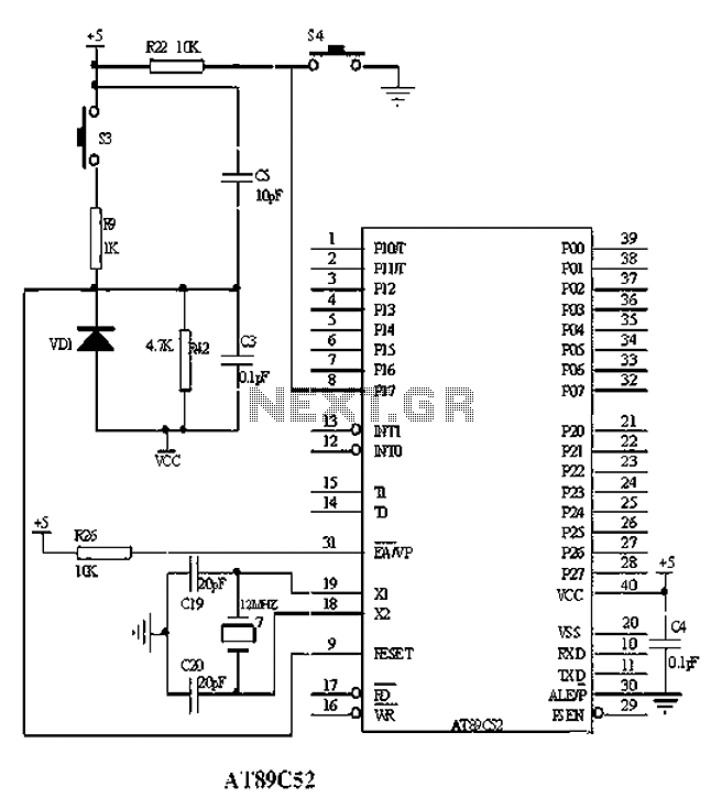
The American Atmel AT89C52 is a low-voltage, high-performance CMOS 8-bit microcontroller chip that contains 8KB of rewritable program memory and 256B of random access data memory (RAM). Atmel's high-density devices utilize non-volatile memory technology and are compatible with the...