
Implementation of Direct Output Buffers
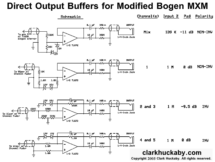
The schematic design comprises six buffer circuits that ensure optimal signal integrity and compatibility with modern audio equipment. Each buffer circuit is meticulously crafted to provide high input impedance, which is essential for maintaining signal quality when interfacing with various audio sources. The low output impedance is crucial for driving longer cable runs without significant signal degradation, making these buffers suitable for both studio and live sound applications.
The use of TL072 op-amps is notable for their low noise and distortion characteristics, which are further augmented by the inclusion of low-noise metal film resistors. This choice of components contributes to the overall fidelity of the audio output, ensuring that the signals remain as true to the original source as possible.
Signal routing within the circuit is designed to maintain consistent polarity, a critical factor in audio processing to avoid phase issues that could lead to undesirable sound artifacts. The careful design of the input and output stages, including the implementation of voltage dividers where necessary, allows for flexibility in interfacing with various audio equipment while preserving the integrity of the signal.
The protective measures implemented, such as zener diodes, reflect a thorough understanding of the operational limits of the components used. This foresight in design helps to prevent damage from unexpected voltage spikes, which can be common in live environments.
Overall, the detailed design of these buffer circuits demonstrates a commitment to high-quality audio performance, with careful consideration given to the electrical characteristics and the physical constraints of the assembly. The integration of modern audio standards ensures that these buffers are well-suited for contemporary applications, providing reliable and high-fidelity audio processing capabilities.A total of six buffer circuits (using three dual op-amp packages), five for the input channels and one for the master output channel. (2) High input impedance (particularly for the five buffers tapping channel faders). (3) Low output impedance (<600 ohm), and stability when driving shielded cables of moderate length. (4) Use of op amps with low noise and distortion and wide bandwidth; use of low-noise metal film resistors throughout. (5) Nominal audio output levels compatible with today`s standard for ground-referenced audio lines, i. e. , -10 dBV (as typified by the Alesis ADAT recorder`s "unbalanced" inputs). (6) Unity voltage gain, and pads (voltage dividers) on inputs where appropriate. (7) Immunity of solid-state devices from damage caused by excessive input voltages. (8) Maintenance of consistent signal polarity from inputs to outputs. (9) All buffers must fit on a perf-board 2. 3 x 3. 7 inches in size, to be located above the chassis plane in a space formerly occupied by two filter capacitor cans.
Figure 10 shows schematics of the four different buffer circuits that I settled on, and photos of their perf-board assembly installed in the MXM are shown in Figure 4. For polarity consistency (specification #8 above), all mic inputs must use today`s standard of XLR pin 2 as "hot" or "+" (where positive voltage swings are analogous to the compression part of a sound wave), with XLR pin 3 as the inverse; on the direct outputs, the signal polarity on the "tip" contact of the 1/4-inch jack should match that of pin 2 on the input XLR.
With two stages of triode amplification, the Channel 1 preamp is a non-inverting amplifier, while each of the other input channels are inverting stages with their single pentodes. Thus, I chose a non-inverting output buffer design for Channel 1 and an inverting design for Channels 2 through 5 ( Figures 10 ).
Relative to the mix bus, the master channel is an inverting amplifier, already compensating for inversion by the majority of the input channels (2 through 5), so I selected a non-inverting buffer to drive the mix output jack ( Figure 10 ). Therefore, signal polarities are consistent throughout, with one exception: the mix output is inverted with respect to Channel 1`s input (as in the original MXM).
All output buffers employ TL072 op amps and share a common capacitor-coupled output design ( Figure 10 ), which uses a 10-microfarad electrolytic capacitor bypassed with a 0. 1-microfarad stacked polypropylene film capacitor. In audiophile circles it`s believed that such bypass capacitors help electrolytics pass high-frequencies and transients, preserving "airiness" in the sound.
From past experience with TL072s used as drivers, I`ve found it important to include the series 100-ohm resistors to insure stable operation into shielded cables under all conditions (especially feeding high-impedance inputs, such as a guitar amp). The 100K resistors further add stability by insuring that all outputs have some pathway to ground regardless of the world external to the MXM.
I bridged the inputs of all buffers with opposing 12-V zener diodes to protect the op amps from instantaneous signal voltages exceeding +/- 12 V ( Figure 10 ). This is a generous margin of safety given +/- 15V operation of the chips. Such overvoltage protection fixes the maximum undistorted output of all six buffers at 18. 6 dBV (= 24 Vp-p); see the gain diagram in Figure 11 ). For the master ("mix") and Channel 1 output buffers, op-amps are configured as simple unity-gain non-inverting voltage followers ( Figure 10 ).
In the master (mix) channel, a voltage divider containing the 100K and 39K resistors forms an 11-dB pad (see section entitled "Pad Decision for the Master Channel Output Buffer"). This sets the input impedance at 139 K-ohm, which is low compared to the other buffers (with their 1 M-ohm input im
🔗 External reference
Related Circuits
40-meter Direct Conversion Receiver. Using the circuit of a 40-meter band direct-conversion receiver described here, one can listen to amateur radio QSO signals in both CW and SSB modes. The 40-meter direct conversion receiver is designed to facilitate the reception...
H66T32BA is a sub-package of H66T19. For a detailed description, please refer to H66T19. The datasheet for H66T32BA can be downloaded from the link provided below. This component is produced by Micro Electronics Ltd. The H66T32BA is a specialized electronic...
The output of the transformer has been calculated to be 125 times higher than the input, based on the ratio of 1000 to 8. Given an input of 12V, the expected output should be 1500V, although there is some...
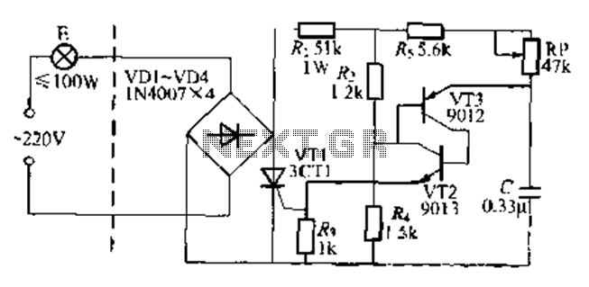
The circuit is a one-way ordinary transistor-triggered dimmer light circuit. It uses a complementary amplifier configuration with transistors VT2 and VT3 to form the thyristor trigger circuit for VT1. The circuit operates with a 220V alternating current through the...
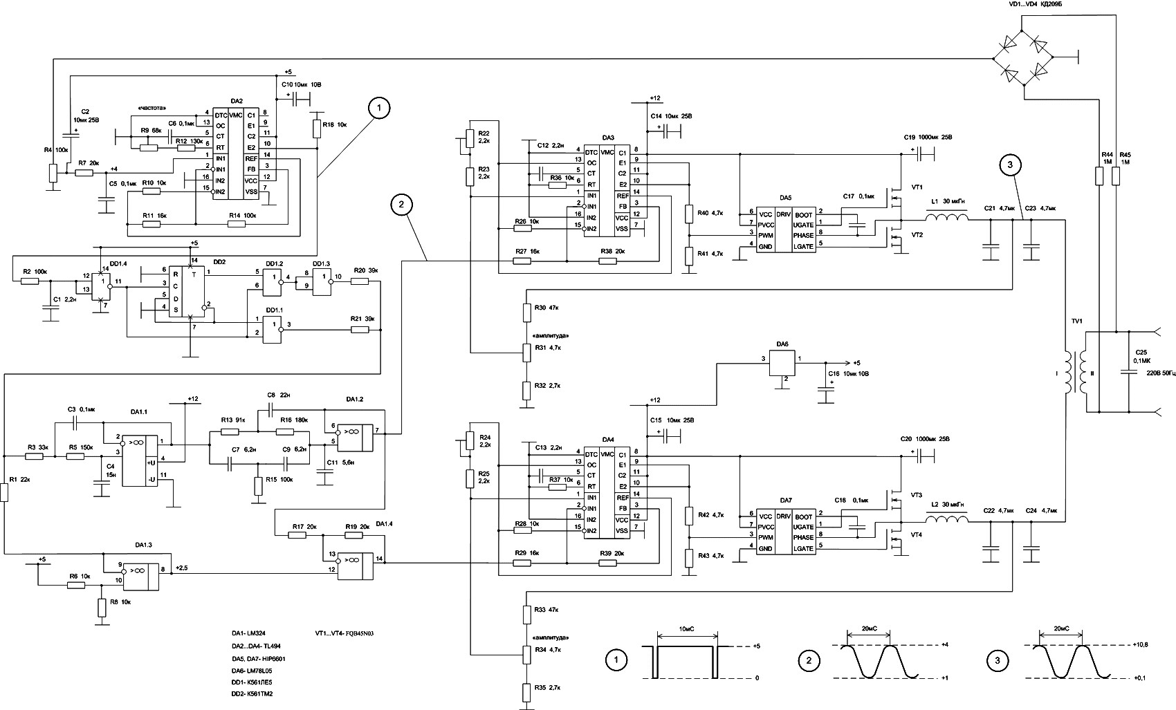
The 50W inverter circuit is built using the power MOSFET FQB45N03 and the IC TL494. This inverter converts a 12-14V DC input from a car battery into a 220V AC output with a 50Hz sine wave frequency. The main...
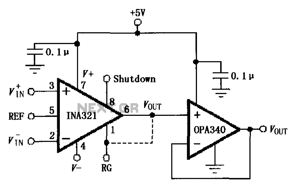
The circuit depicted in the figure consists of an OPA340 operational amplifier configured as a voltage follower, serving as an output buffer for the INA321/322 output. The optimal load impedance for the INA321/322 is 10k ohms or greater. A...
Warning: include(partials/cookie-banner.php): Failed to open stream: Permission denied in /var/www/html/nextgr/view-circuit.php on line 713
Warning: include(): Failed opening 'partials/cookie-banner.php' for inclusion (include_path='.:/usr/share/php') in /var/www/html/nextgr/view-circuit.php on line 713