
IMPROVED REGENERATIVE SW RECEIVER
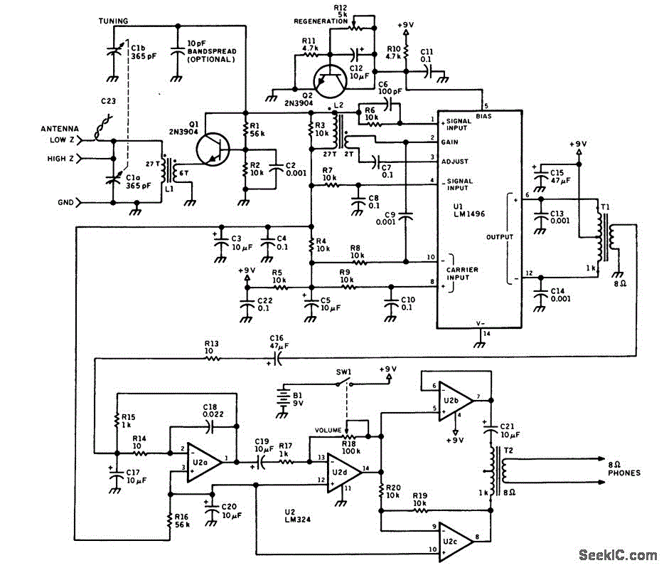
The circuit design showcases a sophisticated approach to regenerative receiver technology, emphasizing stability and sensitivity. The inclusion of a transistor buffer (Q1) effectively mitigates unwanted radiation of oscillator signals, enhancing the overall performance by isolating the antenna preselector from the oscillator circuit. This isolation is crucial in maintaining the integrity of the received signals, especially in environments with varying electromagnetic interference.
The use of the LM1496 as a Hartley oscillator is particularly innovative, as it repurposes the internal components of the IC to create a stable oscillation source. By leveraging the GAIN and ADJUST pins for regenerative feedback, the circuit achieves a high level of sensitivity, making it adept at detecting weak signals. The asynchronous detection capability, facilitated by coupling oscillator output to the CARRIER INPUT, further amplifies the circuit's performance, allowing it to discern signals that might otherwise be lost in noise.
The variable-voltage source created by R12 and Q2 is essential for maintaining consistent performance despite fluctuations in supply voltage. This design choice ensures that the regeneration level remains stable, which is critical for achieving predictable operation in the regenerative feedback loop. The careful design of the emitter output impedance allows for optimal power transfer to the feedback winding, which is a key factor in achieving smooth regeneration control.
The audio output stage, utilizing the LM324 op-amp, provides a robust means of signal amplification, while the push-pull configuration effectively reduces the risk of oscillation in the audio range. This design consideration is vital for high-fidelity audio output, ensuring that the final signal is clean and free from distortion.
Overall, the circuit is well-suited for shortwave reception in the 5 to 15 MHz range, demonstrating a thoughtful balance between complexity and performance. The design choices made reflect a deep understanding of the principles of radio frequency engineering, resulting in a reliable and effective regenerative receiver.The figure shows the schematic of the circuit. A number of unique features give this design its trouble-free performance. The tendency for regenerative receivers to radiate oscillator-frequency signals is eliminated here by placing a transistor buffer Q1 between the antenna preselector circuit L1-C1a and the regenerative oscillator-tuned circuit L 2-C1b. This buffer also nearly eliminates hand-capacitance effects. This design is also unique in that it uses an IC for the regenerative detector. U1, an LM1496 double-balanced mixer, is used here in a somewhat unorthodox manner. The differential SIGNAL INPUT amplifier transistors internal to the IC are used as a Hartley oscillator in conjunction with L2 and C1b. The regenerative feedback for this oscillator is supplied by the output of the GAIN and ADJUST pins of the LM1496.
Some of the oscillator output is coupled to one of the CARRIER IN-PUT pins via C9, which allows the mixer section of U1 to act as an asynchronous detector, greatly improving the RE detection sensitivity over that of other regenerative circuits. The regeneration level is controlled by the voltage level applied to the BIAS pin of U1. The circuit containing R12 and transistor Q2 is used as a variable-voltage source, providing the regeneration level immunity from supply-voltage ripple.
This bias level controls the quiescent current level through the SIGNAL IN-PUT amplifier transistors, which, in turn, determines the emitter output impedance of these transistors, controlling the amount of power delivered to the feedback winding of L2. This results in very smooth and predictable regeneration control. The outputs of U1 are coupled through audio trans-former T1 into the first section of U2, an LM324 op amp.
Volume control is achieved though U2d and variable resistor R18. Using a push-pull audio output stage, as is done here, also reduces susceptibility to audio oscillation. Although the use of switched or plug-in coils could have allowed multiband reception, in the interest of simplicity, this was not done.
However, the values of L1 and L2 allow coverage of 5 to 15 MHz, where much of the shortwave action occurs. 🔗 External reference
Related Circuits
This circuit enables the generation of audio musical notes that can be heard from a distance of up to 10 meters. It consists of two main components: an infrared (IR) music transmitter and an IR music receiver. The IR...

A few weeks ago, Jason NT7S mentioned the ZL2BMI DSB transceiver as a rig that might be of interest for building. He was correct; it had been seen in SPRAT, but for some reason, it had not been seriously...
This GPS receiver is powered by 2 AA batteries. They are only strong enough for the GPS to stay on for about two hours, and this seems like quite a waste. I would like to be able to use...
L1, Q1, L2, and L3 form an RF amplifier stage that drives M1, a doubly balanced mixer. Q4 serves as a local oscillator stage operating in the 375-MHz range. Signals in the 420 to 450-MHz range from Q1 are...
The notch filter can be integrated into nearly any receiver to attenuate a specific frequency by more than 30 dB. This filter is particularly useful for diminishing heterodynes and whistles. A notch filter, also known as a band-stop or band-reject...

The SC1437 is a battery overvoltage detection circuit that includes a driver for an external MOSFET. The trip point can be adjusted using an external resistor divider connected to the SENSE pin. If no external divider is used, the...
Warning: include(partials/cookie-banner.php): Failed to open stream: Permission denied in /var/www/html/nextgr/view-circuit.php on line 713
Warning: include(): Failed opening 'partials/cookie-banner.php' for inclusion (include_path='.:/usr/share/php') in /var/www/html/nextgr/view-circuit.php on line 713