
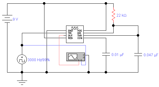
Incorrect frequency from crystal oscillator
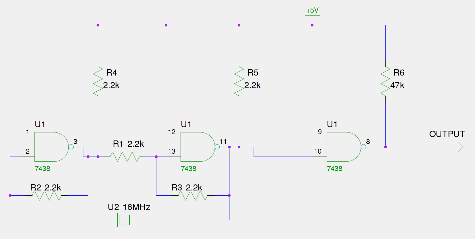
The Eistar SJ-1 digital pulser operates on a frequency generation principle utilizing a Pierce oscillator configuration, which is recognized for its stability and low phase noise characteristics. The Pierce oscillator typically consists of a feedback network that includes a crystal, which defines the oscillation frequency. In this case, the circuit employs a 16 MHz crystal, but the output frequency is measured at 10.6 MHz, indicating a significant deviation from the intended operation.
The presence of the 74LS38 NAND gate suggests that the output stage may be designed to buffer the oscillator output while also providing additional logic functionality. This open collector configuration allows for multiple outputs to be connected, but it also requires careful consideration of pull-up resistors to ensure proper logic levels. The incorrect frequency output could stem from several factors, including the condition of the crystal, the values of the surrounding passive components, and the overall circuit design.
Troubleshooting steps should begin with a thorough inspection of the crystal for any signs of physical damage or degradation, as crystals can fail due to prolonged exposure to high currents or thermal stress. Replacing the crystal with a known good unit can help ascertain if the frequency issue persists. If the crystal is functional, the next step would involve examining resistor R1 and considering the substitution with a capacitor, as the Pierce oscillator typically employs a capacitive element for feedback stabilization.
The design also includes multiple frequency division stages, which could introduce additional sources of error. The 74LS93 and CD4518BE components are integral in reducing the frequency to usable levels, but any misconfiguration or fault in these devices could compound the frequency discrepancy. The multiplexer (74LS151) further complicates the signal path, as it selects between multiple inputs, and any faults in this stage could result in incorrect output frequencies.
Finally, the inductors and resistors present in the circuit may play a role in filtering and impedance matching, and their values should be verified against the design specifications to ensure they are within acceptable tolerances. By systematically addressing each component and stage of the circuit, a resolution to the frequency generation issue can be achieved, restoring the digital pulser to its intended operational state.Acquired an old Eistar SJ-1 Digital pulser. However the frequency it generates is always 66% of what its supposed to produce. Turns out that the frequency coming out of the frequency stage(at Pin 11)is 66% of the 16MHz crystal or about 10. 6MHz. (The 74LS38 is an open collector quad nand gate) I opened it up and traced out the layout. The frequency stage looks like to that I have now learned as a Pierce Type nand gate oscillator. I have drawn an abbreviated schematic of the digital pulser showing the frequency generation stage. In the Pierce type oscillators I have researched, there is a capacitor in between the nand gates where resistor R1 is. However in this design there is a 2. 2k resistor(R1). What could be causing the wrong frequency to be generated How I proceed to troubleshoot and correct the pulser Should I: 1.
Replace the crystal with another and check 2. Replace resister R1 with a capacitor as I have seen in a Pierce type oscillator. I am guessing since the design would have worked at one point in time, R1 is not an issue here. In any case, this circuit looks like it will drive a lot of current through the crystal and the crystal may have been damaged over time as a result. R2 in particular should probably be much larger. Dave Tweed™ Jan 12 `13 at 21:43 66% sounds suspiciously like 2/3. Are you sure there aren`t some multipliers and a PLL in there, and they aren`t set as you think Olin Lathrop Jan 12 `13 at 22:47 2/3 is what I thought too, but I(google) has been unable to find a harmonic for a crystal at 2/3.
Could it be a crystal failure mode For the whole device, the 16MHz from the pierce oscillator feeds into a 74LS93 for a divide by 8, then into three successive CD4518BE for divide by 10 each. All the separate inputs go into a mux (74LS151) which gets selected by the switch and then its back into 74LS93 for a divide by 2.
Finally its buffered through a nand gate in the 74LS38. So no multipliers or PLLs, but there are some 5 band inductors/resistors(blue above) which I have been unable to decipher. Doc Jan 12 `13 at 23:09 🔗 External reference
Related Circuits
A code practice oscillator was built some time ago, and there is a vague recollection of the project. It featured a straight key that plugged directly into the key jack. Upon opening the device, a circuit board populated with...
This report provides details on the principles and operation of an amplifier known as the Wien Bridge Oscillator. The oscillator was designed as part of a laboratory exercise, which was not attended, thus this document will focus on the...
This application note analyzes the details of a Wien-bridge oscillator, shows how a JFET maintains oscillation, and demonstrates adding a digital potentiometer (digipot), rather than a variable resistor, to improve stability and flexibility. The Wien-bridge oscillator is a type of...
The standard assumption is that the phase shift sections operate independently. According to the equation provided, the loop phase shift reaches -180 degrees when the phase shift of each section is 60 degrees. This condition is met when ω...
Signals with a known frequency but an unknown phase can be detected using an in-phase signal and a signal that is shifted by 90 degrees, a method commonly utilized in lock-in amplifiers, synchronous detectors, and frequency-response analyzers. The signal...
This is an operational amplifier (Op-Amp) oscillator circuit. This circuit has several advantages, including its ability to operate at low frequencies. The operational amplifier oscillator circuit is designed to generate a periodic waveform output, typically a sine or square wave,...