
Increase Regulator Voltage Output Schematic Diagram
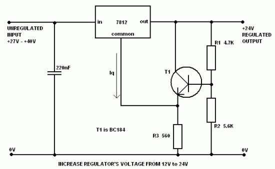
The circuit operates by utilizing a voltage regulator IC whose output voltage is adjusted through an external voltage divider. The common terminal of the regulator is connected to the midpoint of this divider, which typically consists of two resistors, R1 and R2. The voltage at the midpoint is determined by the ratio of these resistors. However, due to the quiescent current from the regulator, the voltage at the midpoint can shift, leading to an unstable output.
To stabilize the output voltage, transistor T1 is introduced into the circuit. This transistor acts as a buffer or an emitter follower, providing a low impedance path at the common terminal of the voltage regulator. By doing so, it minimizes the impact of the quiescent current on the voltage divider. The collector of T1 is connected to the output of the voltage regulator, while the emitter is linked to the common terminal. The base of T1 receives the midpoint voltage from the divider, allowing it to maintain a stable voltage level.
Resistor R3 plays a critical role in this configuration. It connects the emitter of T1 to ground and should be selected carefully. A lower resistance value for R3 ensures that the quiescent current flowing through it does not turn off T1, allowing the transistor to remain active and effectively stabilizing the output voltage. The design ensures that the heat generated is managed efficiently, reducing the risk of thermal issues that could arise from high divider resistor values.
This configuration provides a reliable means of increasing the output voltage of a voltage regulator IC while maintaining stability and efficiency in the circuit operation. The careful selection of resistor values and the incorporation of the transistor buffer enhance the overall performance of the voltage regulation system.It is often necessary to arrange an voltage regulator IC to give a higher output voltage than that set by the regulator alone. One method to achieve this is by connecting the common terminal to the mid-point of a potential divider but the problem with this method is that IC regulators have a small quiescent current (~10mA) flowing out of the co
mmon terminal to ground. The magnitude of this quiescent current is not closely controlled and hence the total output voltage becomes somewhat unpredictable. Low divider resistor values help, but there are likely to be complications of heat dissipation and inefficiency.
The circuit presented here avoids the problem by using the transistor T1 to generate a low impedance at the regulator common terminal by emitter-follow action, while transferring the voltage divider from a relatively high-resistance divider network. The value of R3 is not critical but must be low enough to accept the highest quiescent current without causing T1 to turn-off.
You are reading the Circuits of Increase Regulator Voltage Output And this circuit permalink url it is 🔗 External reference
Related Circuits
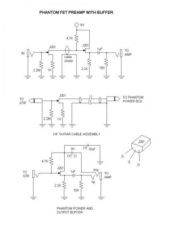
This is a phantom-powered FET preamplifier integrated into a 1/4" guitar cable, similar to the design found on the Tillman site. The amplifier consists of only a few components, making it challenging to trim and solder the leads to...
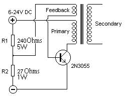
Fully illustrated and schematized plans for a high-performance, easy-to-build transistorized high voltage flyback driver. The high voltage flyback driver circuit is designed to efficiently convert low voltage DC into high voltage pulses suitable for driving flyback transformers. The circuit typically...
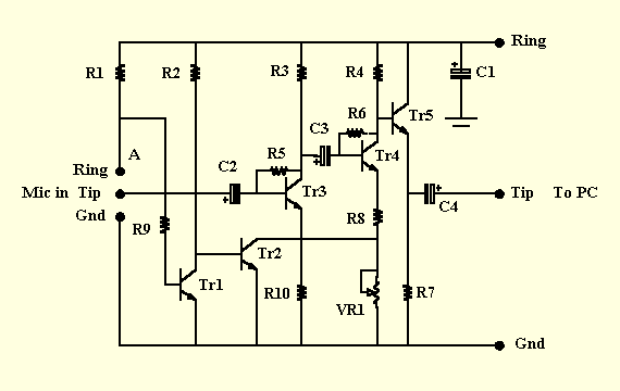
This is a microphone preamplifier designed for compatibility with a SoundBlaster AWE 64 sound card. It is also suitable for any compatible tag or PC audio input that provides a 5 Volt supply through a 2.2kΩ current-limiting resistor located...
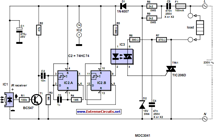
According to the note on the schematic, IC-2 is a 74HC74 TTL chip. Refer to the data sheet for details regarding pins 7 and 14. The note for IC-3, located lower on the schematic, indicates it is an AC...
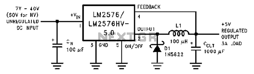
A wide range of 7 to 40V DC-DC step-down circuit that converts input voltage to 5V. This circuit operates as a buck converter, designed to efficiently reduce a higher DC voltage (ranging from 7V to 40V) to a stable output...
The quartz crystal oscillator circuit is highly advantageous in terms of frequency stability. Even the Voltage-Controlled Crystal Oscillator (VCXO) circuit, which allows for significant frequency changes, typically experiences only about a 1% variation. However, the linear range of control...
Warning: include(partials/cookie-banner.php): Failed to open stream: Permission denied in /var/www/html/nextgr/view-circuit.php on line 713
Warning: include(): Failed opening 'partials/cookie-banner.php' for inclusion (include_path='.:/usr/share/php') in /var/www/html/nextgr/view-circuit.php on line 713