
Interfacing LCD via SPI
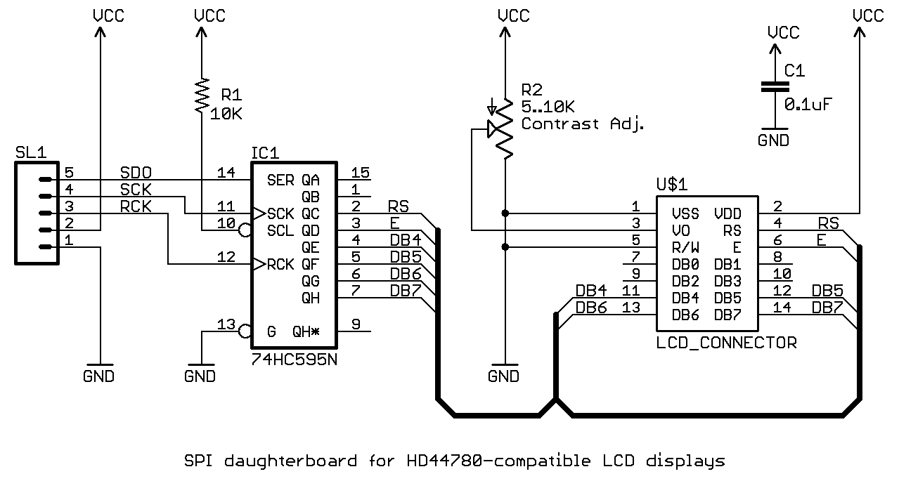
The native LCD interface consists of eight data lines and three control signals, functioning in either 8-bit or 4-bit mode. In 8-bit mode, all data lines are utilized, making LCD control somewhat simpler; however, this mode does not allow for the use of control signals with the shift register. In contrast, 4-bit mode uses only the upper four bits of the data bus, necessitating the division of the data byte into two halves for transmission in two stages. This is the mode selected for implementation. The control signals include RS, RW, and E. The RS signal determines the type of data sent to the LCD: if RS is 0, a command is being sent; if RS is 1, the data represents a character to be displayed. The falling edge of the E signal initiates the transfer of the data bus and RS state to the LCD controller. The RW signal controls data direction; since a unidirectional shift register is used and reading back from the data bus is not possible, RW is connected to ground. In this configuration, instead of reading the LCD state, a sufficient delay is introduced before sending the next byte to the LCD.
The SPI-to-LCD circuit is designed on a small daughterboard that connects to the LCD display, with three signal wires and two power wires linking to the main board with the microcontroller. This daughterboard is intended for attachment to a standard LCD 2G-7 header. A schematic for this design is available, and the board can be ordered from BatchPCB. The main board featuring the microcontroller is kept simple, utilizing the widely-used PIC18F4520 mounted on a breadboard, without requiring a crystal oscillator. The schematic for the breadboard connections is provided. To send a byte to the LCD, the RS signal and the high nibble of the data byte must first be set. Following this, the E signal is activated and then deactivated, allowing the controller to read the data bus on the falling edge of E. Subsequently, the low nibble of the data bus is set, and E is toggled again. A waiting period is necessary before the next byte is transmitted, with the duration of the delay depending on the characteristics of the specific HD44780 LCD being utilized.As time goes by, microcontrollers become more powerful, cheaper, and smaller. A typical micro of the past could have had 40 pins and no internal memory. On the contrary, modern J-series PICs are made with 96K program memory and 28 pins. We can drive a lot of peripherals with that amount of memory, however we are getting short on pins. In this arti cle I will show how to drive a parallel interface peripheral serially. A HD44780-compatible LCD module is good candidate it is popular, inexpensive, and slow, so you won`t be losing any speed while converting parallel to serial. And you could even save some money using a micro with fewer pins. SPI is very easy to implement thanks to synchronous serial communication hardware support in newer PICs.
The only other thing necessary on the LCD end is 74HC595 double-buffered shift register. It can be easily obtained from on-line electronic components distributors, such as Mouser or Digi-Key for as little as 48 cents in SMT package, slightly more in DIP. Since it`s very simple device, most functionality that we need will be done in software. HD44780-compatible LCD (LCD for short) is a parallel device. It has 8 data lines and 3 control signals which tell the controller when data lines contain valid data, what kind of data it is and whether you want to write to the controller or read from it (we won`t be using the last one BTW).
SPI is serial it sends out a byte one bit at a time, marking appearance of each bit with a clock pulse. The 74HC595 receives SPI data and sends is to it`s parallel outputs. Take a look at 74HC595 schematic symbol. It has two buffers one for serial data, another for parallel. Serial data go on pin 14. Serial clock goes on pin 11. When pin 12 goes from low to high serial buffer gets copied to parallel buffer and its contents appear on parallel output pins.
The following animation shows how two bytes 0G—55 ( 0101 0101 ) and 0xAA ( 1010 1010 ), are transferred from SPI to parallel output. Let`s talk briefly about native LCD interface. The device has 8 data lines and three control signals. It can work in either 8-bit or 4-bit mode. In 8-bit mode all data lines are used and LCD control is slightly easier, however, if we utilize this mode our little shift register won`t be able to accommodate any of the control signals.
In 4-bit mode only upper 4 bits of the data bus are used; the data byte needs to be split in two halves and sent in two transfers. This is the mode that we will be using. Control signals are RS, RW, and E. RS defines what kind of data is being sent to LCD. If RS is 0, we are sending a command, if RS is 1, the data is just a character to be printed on the screen.
Falling edge of E initiates transferring of data bus and RS state to LCD controller. The last signal is RW it controls data direction. Since we are using unidirectional shift register and won`t be able to read back the data bus, RW is simply tied to ground. In this mode, instead of reading LCD state we will just wait long enough before sending next byte to LCD.
The SPI-to-LCD circuit is made on a little daughter board. The idea is to attach it to LCD display and have 3 signal and 2 power wires run to the main board with MCU. The daughter board is designed to be attached to standard LCD 2G—7 header. Here is a schematic. The board is available to order at BatchPCB To keep you focused on communication with LCD the main board with MCU is made very simple.
It`s ever-popular PIC18F4520 mounted on a breadboard. No crystal oscillator is used. Here is a schematic of breadboard connections. What do we need to send a byte to LCD First, RS and high nibble of data byte needs to be set. Then, E needs to be set and cleared controller reads data bus on the falling edge of E. After that, we need to set low nibble of data bus and toggle E again. We need to wait some time before sending next byte. The delay depends on characteristics of the specific HD447 🔗 External reference
Related Circuits
SPI Integrated Circuit Bus, IC Buses, an IC, Chip-to-Chip Bus Serial Peripheral Interface, Integrated Circuit Bus types, and IC Bus Electrical Interface Descriptions. Peripheral Interface (SPI) circuit is a. The Serial Peripheral Interface (SPI) is a synchronous serial communication...

This add-on device for telephones can be connected in parallel to the telephone instrument. The circuit provides audio-visual indication of on-hook, off-hook, and ringing modes. It can also be used to connect the telephone to a CID (caller identification...
There are two primary types of backlights for LCDs: LEDs, which stands for light-emitting diodes, and EL, which stands for electroluminescent. EL backlights are generally more efficient and provide more uniform lighting compared to LED backlights, but they require...
The RF module operates at radio frequencies, with a frequency range between 30 kHz and 300 GHz. In this RF system, digital data is represented as variations in the amplitude of a carrier wave, a modulation technique known as...
Function: Used to measure the voltage change minute by management before the temperature diodes. Component: IC, Diode, Resistor, 3-1/2 digit LCD (SP521PR). The circuit described functions as a voltage measurement system designed to monitor minute voltage changes, particularly in relation...
This project involves an output port expander for the 8051 microcontroller. It focuses on interfacing a large load bank with the microcontroller. In this load bank project, up to 50 solid-state relays are connected to the microcontroller using the...