
inverter circuit diagram
The described DC-AC power converter circuit utilizes a topology that is widely recognized for its efficiency and effectiveness in transforming direct current into alternating current. The circuit features a pair of transistors that operate in a complementary fashion, effectively controlling the flow of current through the center-tapped winding of a step-up transformer. This configuration allows the circuit to boost the voltage level while converting the DC input.
The PCB layout includes detailed representations of both the top and bottom copper layers, providing a comprehensive view of the circuit's design. The six large pads located at the edges of the board are specifically designed for mounting screws, ensuring that the control board is securely fixed within its enclosure.
In the schematic, discrete components such as resistors, capacitors, and diodes are strategically placed to facilitate various functions, including filtering, voltage regulation, and signal conditioning. Each component's placement is critical for the overall performance and stability of the inverter circuit. Furthermore, integrated circuits (ICs) on the board are responsible for specific tasks, such as control logic and signal processing. The square pad marking pin number 1 on each IC assists in proper orientation and connection during assembly.
This detailed layout and component arrangement are essential for achieving optimal performance in the inverter circuit, ensuring reliable operation in applications where DC to AC conversion is required. The design and implementation of such circuits are crucial in various fields, including renewable energy systems, power supplies, and motor drives.A common topology for DC-AC power converter circuits uses a pair of transistors to switch DC current through the center-tapped winding of a step-up transformer Examine these checkplot images from a PCB drafting program, for a control board based on this inverter circuit design. Both the top and bottom copper layer plots are shown from the perspect ive of the board`s top side. The six large pads around the periphery of the board are actually holes for mounting screws Mark where discrete components (resistors, capacitors, and diodes) go into the PCB, and identify which integrated circuits on the board layout are performing which functions in the schematic. Note: the square pad on each IC marks pin number 1 🔗 External reference
Related Circuits
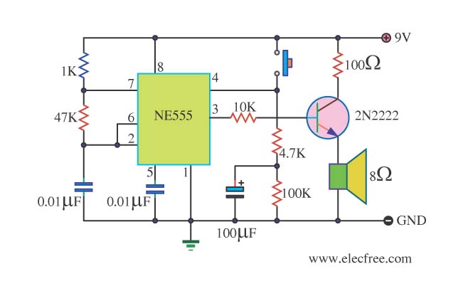
This is a danger beep circuit. It uses a 555 integrated circuit configured as a stable multivibrator that provides a duty cycle of 5% to drive a loudspeaker. The danger beep circuit utilizes the 555 timer IC, a versatile and...

A capacitor step-down DC power supply circuit is presented. This circuit eliminates the need for power transformers, utilizing capacitive voltage drop rectification and regulation, which significantly reduces the overall size of the circuit. The circuit includes a capacitor step-down...
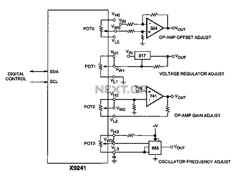
A XICOR X9241 POT IC module can be utilized to modify the four digital analog circuits, as depicted in the schematic. The XICOR X9241 is a digital potentiometer integrated circuit designed for precise adjustment of analog signal levels in various...
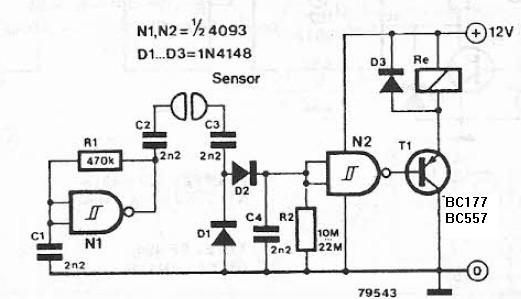
The liquid detector is a device designed to detect the presence of liquid using alternating voltage. This circuit can be constructed using common electronic components. The alternating voltage is generated by a gate with a Schmitt trigger function, acting...
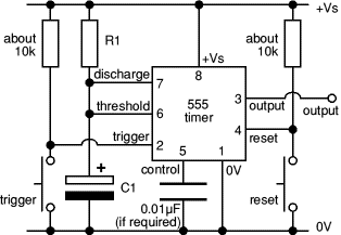
The 8-pin 555 timer is one of the most versatile integrated circuits (ICs) available, utilized in numerous projects. With minimal external components, it can be employed to construct various circuits, many of which do not pertain to timing applications....
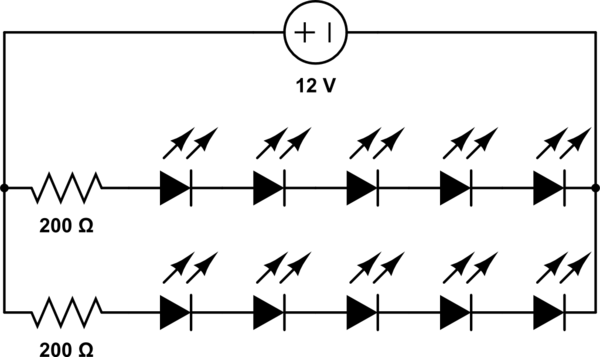
A 12V power supply is available, and there is a need to power LEDs with a forward voltage of 2V. It is questioned whether only six LEDs can be powered or if the cathode of one LED can be...