
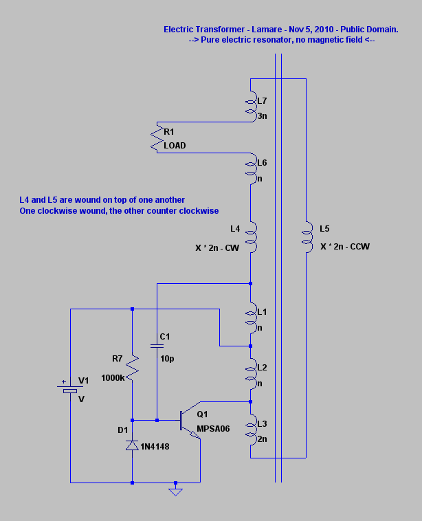
Kapagen Generator
The described circuit utilizes bifilar winding techniques to exploit parasitic capacitance, which plays a crucial role in energy storage and oscillation enhancement. The bifilar winding creates two closely spaced conductors that can store energy in their mutual capacitance, thereby increasing the effective voltage difference between adjacent windings. This method allows for a more efficient energy transfer during resonance, where the alternating energy between capacitance and inductance can amplify oscillatory behavior.
In the context of Tesla's design, the series connection of the windings allows for a uniform voltage distribution across the coil, which is beneficial for applications requiring consistent output. Conversely, the Kapagen device's CW and CCW winding arrangement potentially offers advantages in terms of voltage variation along the coil length, which may enhance performance in specific applications such as energy harvesting or resonant energy transfer.
The implications of using different lengths of short coils in the Kapagen device suggest a novel approach to tuning the resonant frequencies and harmonics, allowing for fine-tuning of the circuit's performance. This configuration may enable the generation of higher harmonics while maintaining the desired voltage gain, which is a critical factor in many high-frequency applications.
The proposed dual-layer coil design, consisting of one layer wound in a clockwise direction and the other in a counterclockwise direction, aims to mitigate the cancellation of magnetic fields observed in Tesla's winding method. By ensuring that the currents in each layer flow in opposite directions, the design seeks to maintain a stable electric field across the windings while minimizing magnetic interference. This innovative approach could lead to more efficient energy conversion and improved performance in devices utilizing these winding techniques. Overall, the integration of these principles into electronic schematics provides a foundation for developing advanced circuits that leverage resonance and capacitance for enhanced energy management.The principle is that there is a certain parasite capacitance between coil windings, which stores a certain amount of energy. By winding the coil bifilar, you get substantial bigger voltage differences between adjacent windings and therefore more energy is being stored in these parasite/self capacitances.
Since the energy stored in a capacitor equ als 1/2 C V ( Energy Stored on a Capacitor ), this is a significant difference in the amount of energy that is being stored in the coils self capacitance. And since in resonance, this energy is being flipped back and forth between the capacitance (voltage) and the inductance (current, magnetic component) you get significantly stronger oscillations in there.
What is interesting is to compare Tesla`s bifilar wound coil from his patent with the top/bottom coils in the Kapagen device. As you can see, Tesla connected them in series, in order to get the voltage difference, while in the Kapagen device they are wound CW/CCW.
So, with Tesla`s coil, the voltage difference between adjacent windings is distributed across the coil, while with the Kapagen device, this increases from top (connected part) to bottom. Given that with the Kapagen device, we have different length short coils at the top and the bottom, this suggests that you probably may use this principle also at higher harmonics with the Kapagen way of winding and still get this voltage gain effect.
You see, with Tesla`s way of winding, you only get the situation that the magnetic field caused by the currents trough each half of the coil cancel each other out at the half wave resonance frequeny (over the whole coil), while with Kapagen`s, they seem to always( ) cancel one another out, or at least at more than one higher harmonic. So, it seems that with Kapagen`s way of winding, you can create a pure (longitudinal, "pressure-like") electric oscillation across the coil windings, without creating a magnetic field.
Based on that, I came on this idea to use a dual layer coil, with one layer wound clockwise and the other counter clockwise, which would be L4/L5 in this schematic: 🔗 External reference
Related Circuits
This design outlines a simple 1 kHz square wave generator utilizing a few components and the LM3909 integrated circuit, which is beneficial for testing audio equipment. The circuit operates on a single 1.5V battery cell, producing a maximum output...
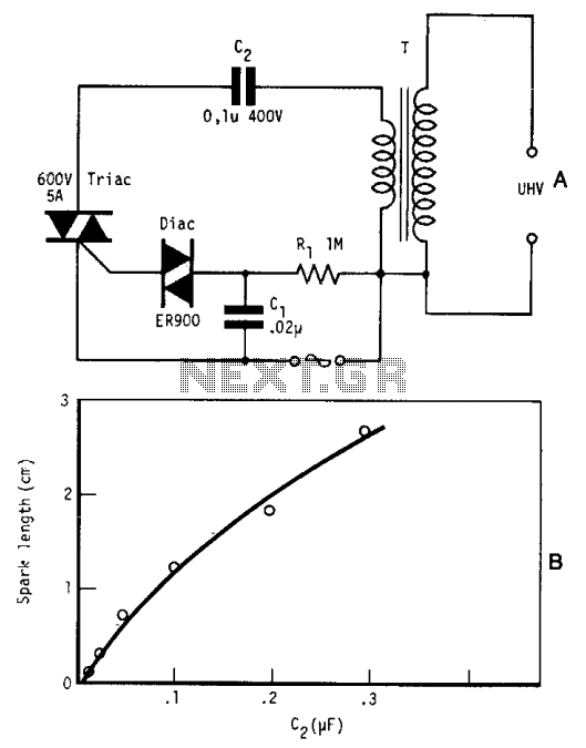
By repetitively charging and discharging a capacitor through the primary winding of an induction coil with high voltage, an ultra-high electromotive force (emf) is induced in the secondary winding. Switching is performed by a triac, which is triggered by...

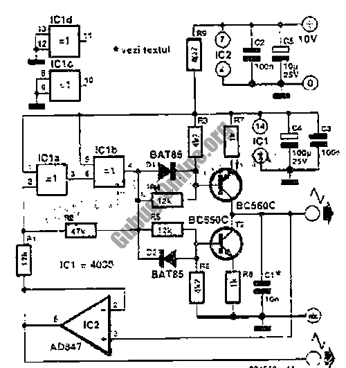
This circuit represents a waveform generator, which is highly beneficial for electronic experiments and design. It primarily generates sine wave oscillations, but the circuit can be modified to produce triangle or square wave functions. The circuit is based on...
Three circuit options Can be synchronized to Christmas tree flashing lights This circuit generates a dual-tone bells ringing similar to most door-bell units. It can be used in many applications other than door-bell. In the Notes below several options...
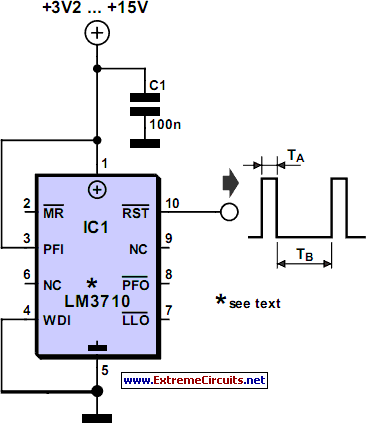
A rectangular-wave pulse generator with an extremely long period can be constructed using only two components: a National Semiconductor LM3710 supervisor integrated circuit (IC) and a 100-nF capacitor to suppress noise spikes. This circuit leverages the watchdog and reset...
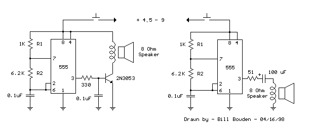
This is a basic 555 square wave oscillator designed to generate a 1 kHz tone for an 8-ohm speaker. In the circuit, the speaker is isolated from the oscillator by an NPN medium power transistor, which supplies more current...