
Klee Sequencer Circuit Theory of Operation
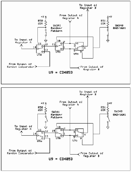
The circuit design integrates a CD4013 dual D-type flip-flop to manage the loading and clocking operations of the shift registers. The CD4013’s first section is pivotal in toggling between serial and parallel modes, dictated by the PSA signal. In serial mode, the shift registers sequentially process incoming data, while in parallel mode, they capture multiple bits simultaneously based on the configuration from external switches.
The R Async signal serves a critical role in synchronizing the loading process. The timing of R Async is crucial as it determines when data is latched into the shift registers, ensuring that transitions occur cleanly without data loss. The use of capacitors C9 and C18 introduces necessary delays and stabilization in the signal transitions, preventing unintended glitches that could disrupt the operation.
The manual load switch provides an alternative means to initiate the load function, enhancing the circuit's flexibility. The debounce capacitor C11 ensures that mechanical noise from the switch does not cause multiple spurious triggers, thus maintaining signal integrity.
In summary, this circuit efficiently manages data loading and processing through well-timed control signals, allowing for seamless operation between parallel and serial modes. The design is robust, leveraging common components to achieve functionality that is both reliable and adaptable to various input signals.Clock and Load functions, with Load being the first function described. U5, CD4013, performs the load function by controlling whether the shift register ICs are in the parallel or serial mode. For 99. 99% of the time, the shift registers are in the serial mode. In the serial mode, each shift register will cycle bits through the register, left to right. With each clock pulse, the bit present on the serial input of the shift register will enter the shift register, and the bit present in the eighth position of the shift register will pass out of the shift register. In the parallel mode, each shift register will "look at" the bits programmed on its parallel inputs. The pattern switches set these bits. The switch to and from the parallel mode is a very fast operation - this mode looks at the bit pattern programmed by the pattern switches only long enough to load the data, then the shift registers revert back to serial mode.
Two shift register control signals are generated by U5. When the PSA signal goes high, it puts the shift registers in the serial mode. Immediately afterwards, the R Async signal goes high. When R Async goes high, it clocks the parallel data into the shift registers on its rising edge. Nearly as soon as it goes high, R Async goes low, which in turn causes PSA to go low, which puts the shift registers back in serial mode. The CD4013 calls these shots, and it is told to do so by the rising edge of a pulse applied to the clock pin of its first stage (pin 3).
There are three events that can produce this triggering event: The rising edge of the signal applied to U5, pin 3, clocks the first section`s Q signal (pin 1) high. This pulls the PSA signal high. When PSA is high, the two shift register ICs are put into the parallel mode. When PSA ("Q" pin 1 of U5) transitions from low to high, the rising edge of this signal clocks the second stage of U5, because this signal is also connected to the clock input of the second section (pin 11).
Clocking the second section of U5 causes its Q signal to go high (pin 13). This creates a sharp rising pulse, which pulls the signal R Async high. The transition of R Async from low to high clocks the parallel data into the shift register ICs. When R Async goes high (Q of the second section), this signal is squared up by R22/D3 and slightly delayed by C9. When it pulls high enough, this signal resets the second section of U5, because it is fed into the reset pin (pin 10).
Resetting the second section brings Q of the second section low, causing R Async to go low again. This transition also briefly pulls the voltage of pull-up resistor R20 low through C18. When this signal goes low, it causes the output of U2, Pin 8 to create a positive going pulse. This pulse is applied to the reset pin of the first section of U5 (pin 4), which pulls PSA low, placing the shift registers back into the serial mode. U5 is then ready to complete the operation again whenever the next load pulse is received. Manual Load Switch: When the manual load switch is pressed, R27 is pulled low, which causes the voltage of R18 to pull low briefly through through C11, the "debounce" capacitor.
When R27 is pulled low, it pulls pin 5 of U2 low, which causes pin 6 of U2 to snap high. This signal is ORed by U3 (pin 2) with any pulse that may be generated by the external load input, which would be present on pin 1 of U3. The output of this section of U3 is applied to pin 8 of U3, where it is ORed with any Gate Bus 1 signal that may be present on pin 9 of U3, and the signal is passed from pin 10 of U3 to the clock input of the first section of U5 (pin 3).
External Load Input: Signals applied to the external load input fi 🔗 External reference
Related Circuits
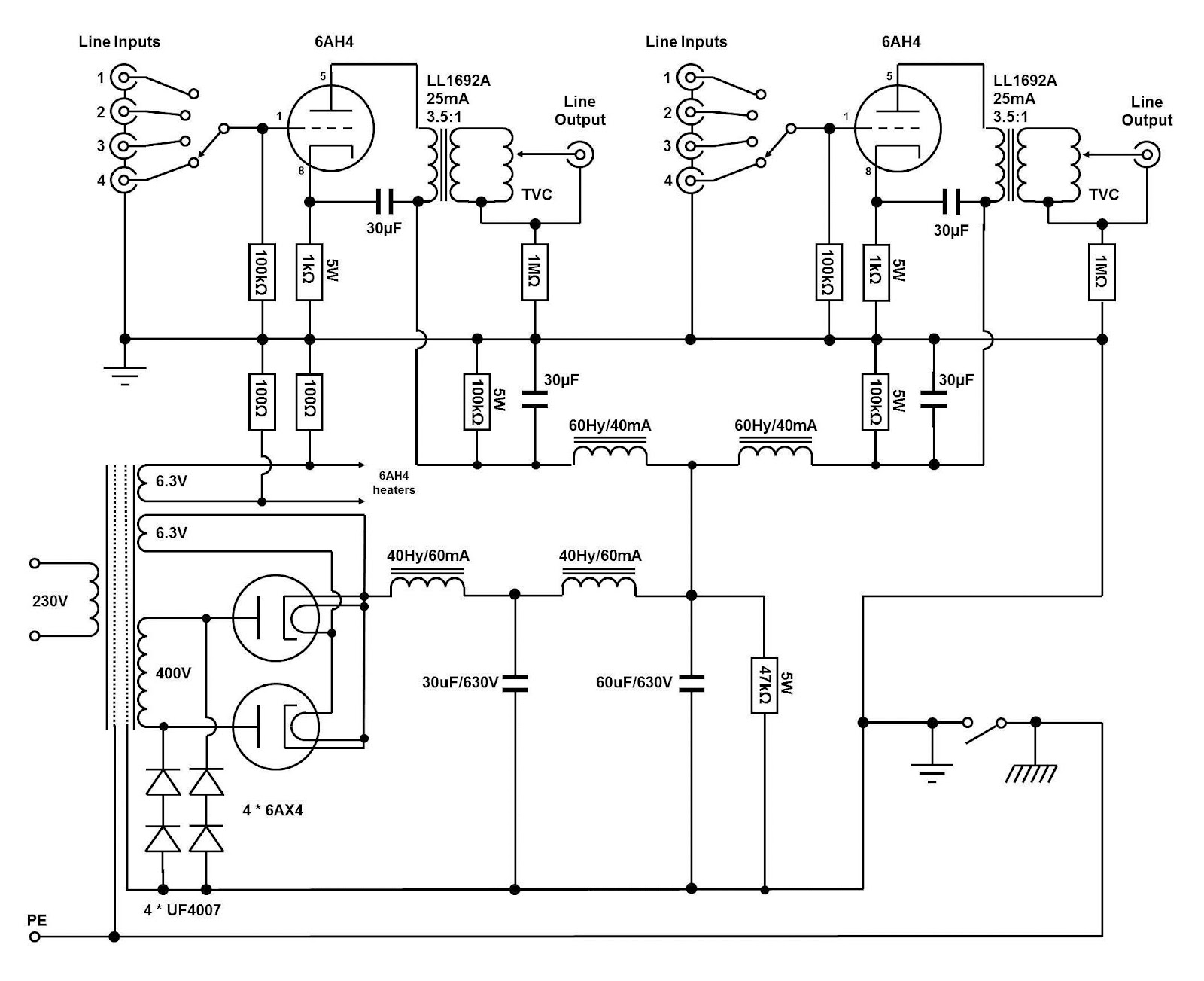
The circuit and assembly process of the line stage is presented in two separate articles. This linestage shares the same circuit as the two chassis version previously described. However, in this design, the power supply and preamplifier are housed...
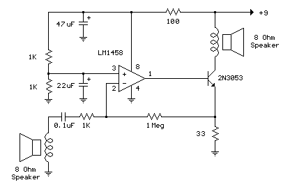
The example below illustrates using an op-amp as an audio amplifier for a simple intercom. A small 8 ohm speaker is used as a microphone which is coupled to the op-amp input through a 0.1uF capacitor. The speaker is...
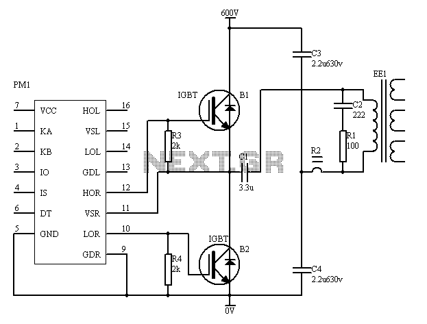
The PM4040F is utilized in switching power supply applications for medium power ranges. It is designed to drive power supplies between 200W and 800W, as illustrated in the accompanying bridge circuit. For power applications below 1000W, an alternative circuit...
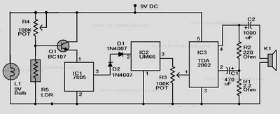
When there is no smoke, the light from the bulb directly illuminates the Light Dependent Resistor (LDR). In this condition, the resistance of the LDR is low, resulting in a voltage drop of less than 6V across it. Consequently,...
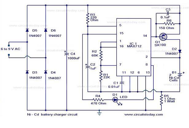
The following circuit illustrates a super fast Ni-Cd battery charger. It is based on the IC MAX 712 and is designed to charge a Ni-Cd battery at a rate of 300 mA. The circuit utilizes the MAX 712 integrated circuit,...
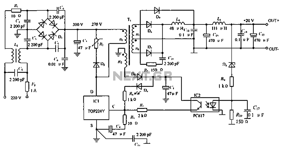
The circuit depicted in the figure is designed to achieve a higher power output by modifying specific components. On the left side of the figure, components R1, L1, D1, and capacitors C1 to C7 form a conventional filtering and...
Warning: include(partials/cookie-banner.php): Failed to open stream: Permission denied in /var/www/html/nextgr/view-circuit.php on line 713
Warning: include(): Failed opening 'partials/cookie-banner.php' for inclusion (include_path='.:/usr/share/php') in /var/www/html/nextgr/view-circuit.php on line 713