
LF356 composed of AD converter
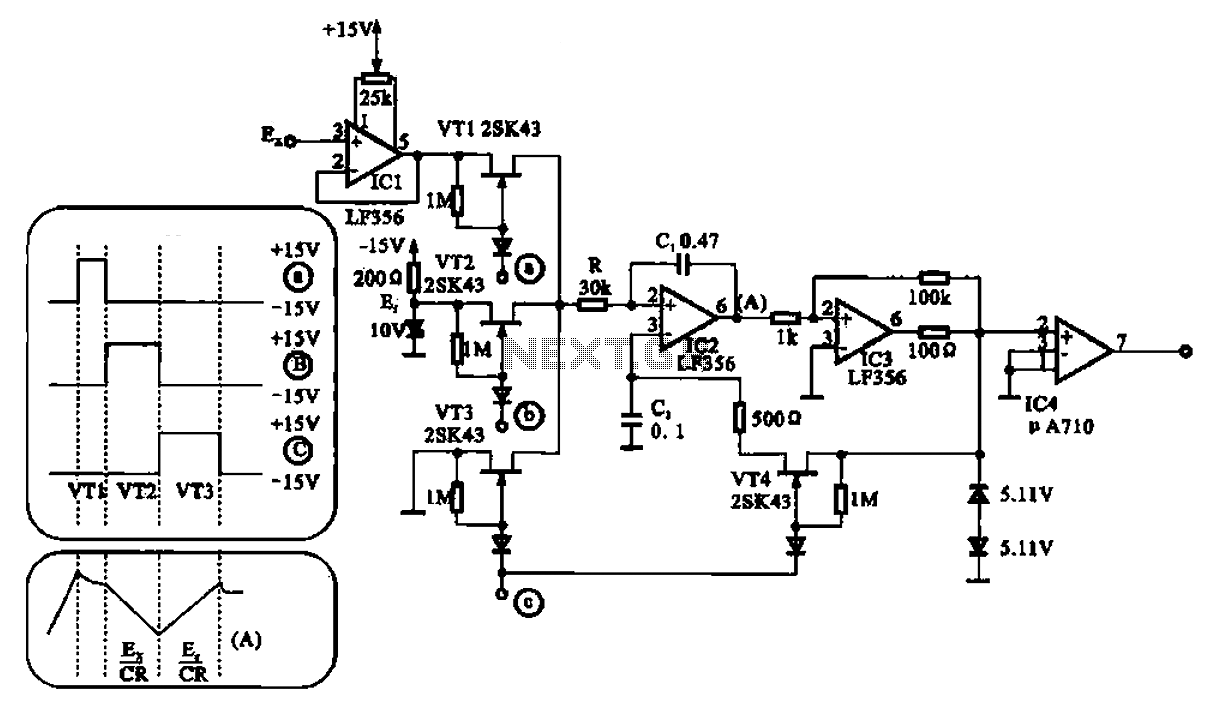
The A/D converter is an essential component in modern electronics, enabling the interface between analog signals, such as those from sensors, and digital systems, such as microcontrollers and digital signal processors. The LF356, a quad operational amplifier, is often employed in A/D converter designs due to its high-speed performance and low noise characteristics, making it suitable for applications requiring precise signal conversion.
In a typical A/D converter circuit utilizing the LF356, the analog input signal is first conditioned through amplification and filtering stages to ensure that it falls within the acceptable input range of the converter. The LF356 can be configured as a non-inverting amplifier to boost the signal amplitude while maintaining its integrity.
The output from the LF356 is then fed into a sample-and-hold circuit, which captures the analog signal at a specific moment in time, allowing for accurate conversion. This is crucial in applications where the input signal may vary rapidly. Following the sample-and-hold stage, the signal is directed to the A/D conversion stage, which employs techniques such as successive approximation, flash conversion, or delta-sigma modulation, depending on the design requirements.
The choice of A/D conversion technique affects the speed, resolution, and overall performance of the circuit. For instance, a successive approximation A/D converter might be chosen for its balance between speed and resolution, while a flash converter might be preferred for applications requiring extremely fast conversion times.
The output of the A/D converter is a digital representation of the analog input signal, which can then be processed by digital circuits. Proper layout and design considerations are critical to minimize noise and ensure signal integrity throughout the conversion process. Additionally, decoupling capacitors and careful grounding techniques should be implemented to enhance performance and reliability of the A/D converter circuit.A/D converter is the analog signal into a digital circuit, it has a variety of circuits, as shown in Figures 21-24 is a circuit A/D converter structure, which is the use of a p ractical circuit configuration of the integrated circuit LF356 .
Related Circuits
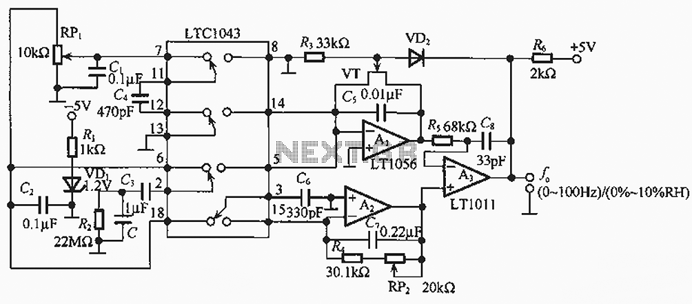
The humidity/frequency conversion circuit operates similarly to the previously mentioned humidity sensors. At a humidity level of 76%, the equivalent capacitance is 500 pF, with a capacitive relative humidity variation rate of +1.7 pF/%. The circuit includes an integrating...
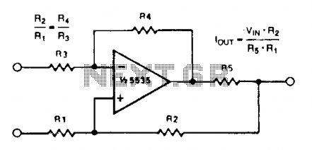
A simple voltage-to-current converter is illustrated. The output current is given by 0t or Vjn/R. For negative currents, a PNP transistor can be employed, and for improved accuracy, a Darlington pair can replace the transistor. With meticulous design, this...
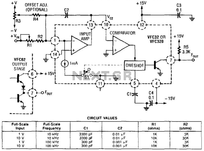
This voltage-to-frequency converter utilizes a Burr-Brown VFC 32 integrated circuit (IC) and requires minimal components. The circuit values are illustrated in the accompanying figure. This charge-balanced voltage-to-frequency (V/F) converter employs either a VFC32 or a VFC320 IC. The positive...
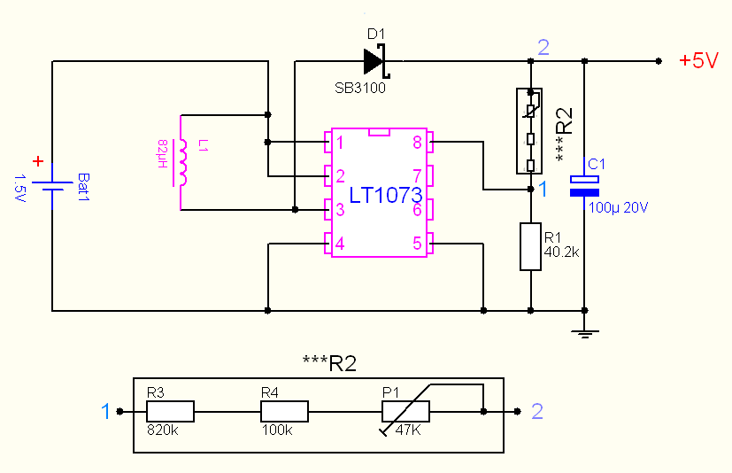
A compact DC/DC converter designed to provide either 5V or 12V output using the LT1073 integrated circuit (IC). This IC is available in three versions based on the desired output voltage, with two options providing fixed outputs of 5V...
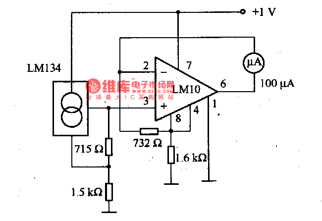
This is an electric thermometer circuit composed of the LM134. In the circuit, the voltage or current output by the LM134 is proportional to the thermodynamic temperature, which can be read on a 100 µA meter. The test temperature...
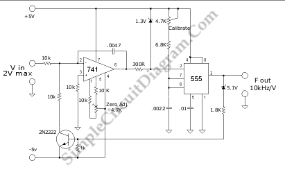
A voltage-to-frequency converter (VFC) circuit is illustrated in the schematic diagram below. The circuit utilizes a 555 integrated circuit (IC) as the central component of its operation. The voltage-to-frequency converter (VFC) is a crucial electronic circuit that converts an input...