
Linear MOSFET voltage regulator
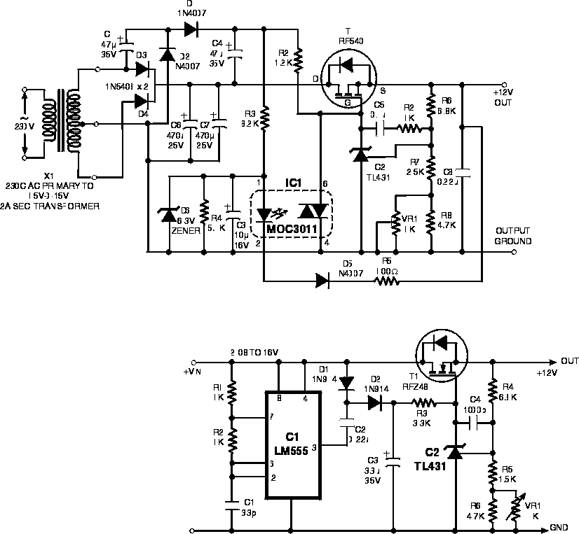
The circuit operates as a linear voltage regulator utilizing a MOSFET, specifically the IRF540, which is capable of providing a regulated output voltage of 12V with minimal voltage drop, particularly advantageous in low-power applications. The design incorporates a step-down transformer with a secondary output of 15V-0-15V, which is rectified to produce a DC input voltage. The gate drive for the MOSFET is generated by a voltage doubler circuit formed by diodes D1 and D2 in conjunction with capacitors C1 and C4, ensuring that the gate voltage is sufficiently above the source voltage to fully turn on the MOSFET.
The adjustable shunt regulator TL431 functions as an error amplifier, monitoring the output voltage and adjusting the gate voltage dynamically to maintain regulation. A trimpot (VR1) allows for fine-tuning of the output voltage, ensuring precise control over the voltage level provided to the load. Capacitor C5 and resistor R2 work together for compensation of the error amplifier, enhancing stability and transient response.
To protect the circuit from potential damage during short-circuit conditions, a crow-bar protection mechanism is implemented. Under normal conditions, diode D5 remains off, but during a short-circuit event, the output voltage drops, allowing D5 to conduct and trigger the opto-triac MOC3011. This action pulls the gate voltage to ground, effectively limiting the output current and protecting the components. The circuit remains in this protective state until the input voltage is removed and reset.
An alternative configuration utilizes an LM555 timer as a charge pump to generate the gate voltage from a DC rail, providing flexibility in the power supply design. This approach allows the circuit to operate efficiently at lower input voltages, further minimizing power loss and improving overall performance. The design considerations, including the selection of low RDS(on) MOSFETs and the potential for paralleling multiple devices, contribute to enhanced efficiency and reduced thermal management requirements.The circuit is a MOSFET based linear voltage regulator with a voltage drop of as low as 60 mV at 1 ampere. Drop of a fewer millivolts is possible with better MOSFETs having lower RDS(on) resistance. The circuit in Fig. 1 uses 15V-0-15V secondary from a step-down transformer and employs an n-channel MOSFET IRF 540 to get the regulated 12V output from DC input, which could be as low as 12.06V.
The gate drive voltage required for the MOSFET is generated using a voltage doubler circuit consisting of diodes D1 and D2 and capacitors C1 and C4. To turn the MOSFET fully on, the gate terminal should be around 10V above the source terminal which is connected to the output here.
The voltage doubler feeds this voltage to the gate through resistor R1. Adjustable shunt regulator TL431 (IC2) is used here as an error amplifier, and it dynamically adjusts the gate voltage to maintain the regulation at the output. With adequate heatsink for the MOSFET, the circuit can provide up to 3A output at slightly elevated minimum voltage drop.
Trimpot VR1 in the circuit is used for fine adjustment of the output voltage. Combination of capacitor C5 and resistor R2 provides error-amplifier compensation. The circuit is provided with a short-circuit crow-bar protection to guard the components against over-stress during accidental short at the output. This crow-bar protection will work as follows: Under normal working conditions, the voltage across capacitor C3 will be 6.3V and diode D5 will be in the off state since it will be reverse-biased with the output voltage of 12V.
However, during output short-circuit condition, the output will momentarily drop, causing D5 to conduct and the opto-triac MOC3011 (IC1) will get triggered, pulling down the gate voltage to ground, and thus limiting the output current. The circuit will remain latched in this state, and input voltage has to be switched off to reset the circuit.
The circuit shown in Fig. 2 follows a similar scheme. It can be utilised when the regulator has to work from a DC rail in place of 15V-0-15V AC supply. The gate voltage here is generated using an LM555 charge pump circuit as follows: When 555 output is low, capacitor C2 will get charged through diode D1 to the input voltage. In the next half cycle, when the 555 output goes high, capacitor C3 will get charged to almost double the input voltage.
The rest of the circuit works in a similar fashion as the circuit of Fig. 1. These circuits above will help reduce power-loss by allowing to keep lower input voltage range to the regulator during initial design or even in existing circuits. This will keep the output regulated with relatively low input voltage compared to the conventional regulators.
The minimum voltage drop can be further reduced using low RDS(on) MOSFETs or by paralleling them. 🔗 External reference
Related Circuits
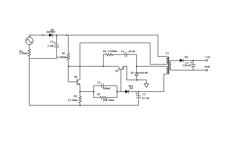
An old Nokia phone charger with a 5.6 V output was modified to provide 12 V by changing the Zener diode from a 9.1 V to a 16 V component. The circuit is mostly understood, but clarification is needed...
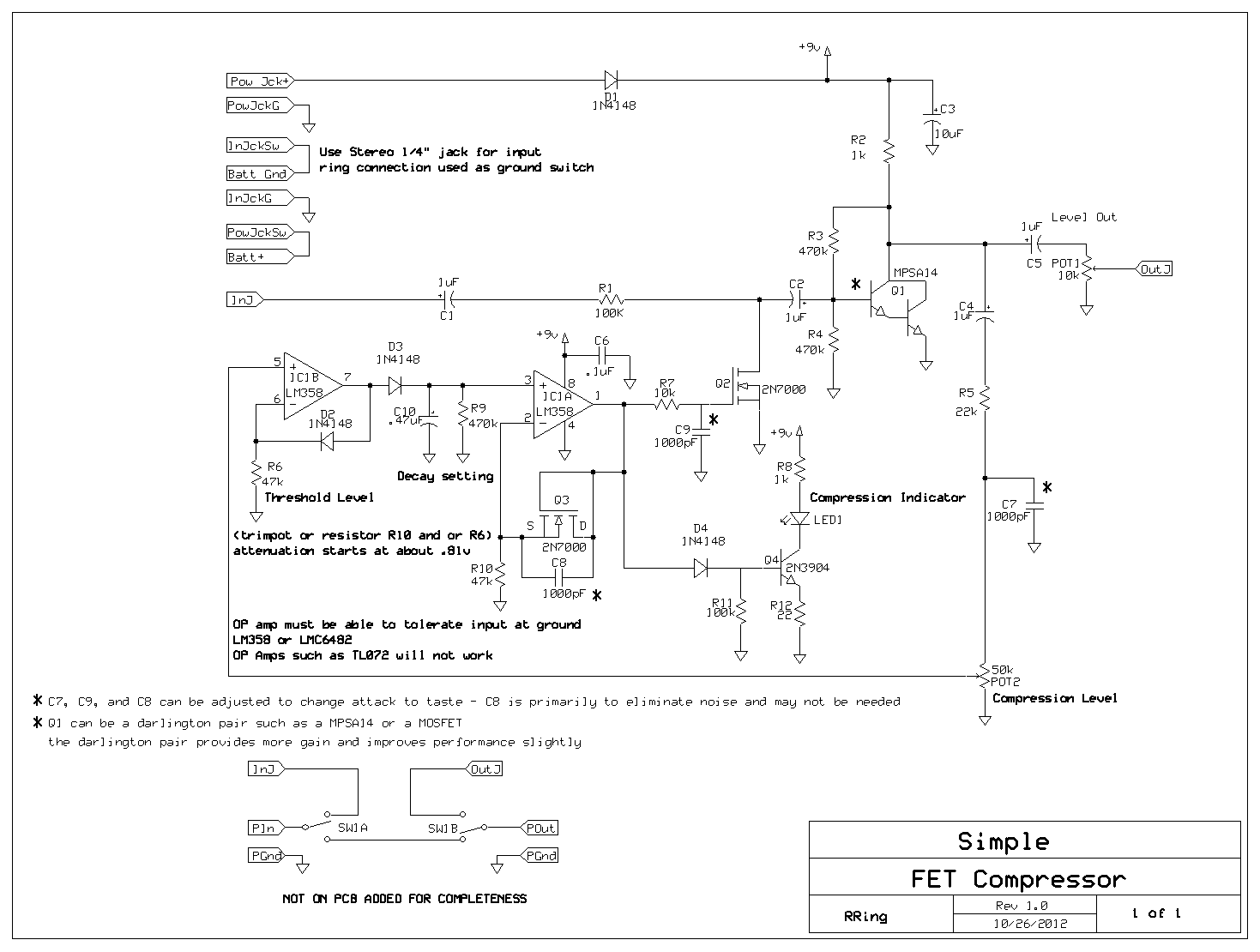
Here is a link to the ExpressPCB layout for this compressor. If you are not familiar with ExpressPCB, look it up. They provide a layout tool that is very easy to use, and you can have boards manufactured for...
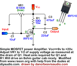
A new enthusiast in electronics has recently taken up the hobby, having built a few guitar pedals and small amplifiers. The current project involves a new electronic device. The project may involve designing a circuit that incorporates various components typical...
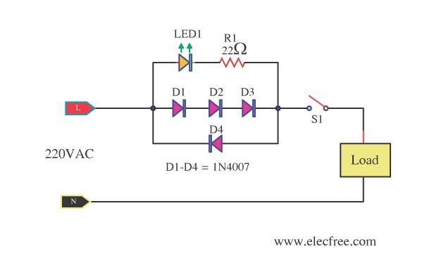
A need exists for a 220V AC line light display or main voltage monitor due to frequent electrical issues in a home. To create a 220V AC line light display or voltage monitor, a circuit can be designed using a...
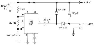
This voltage doubler circuit utilizes a 555 timer integrated circuit configured as an astable multivibrator. It can deliver a maximum output current of 50mA; exceeding this limit will result in a reduction of the output voltage. The actual output...
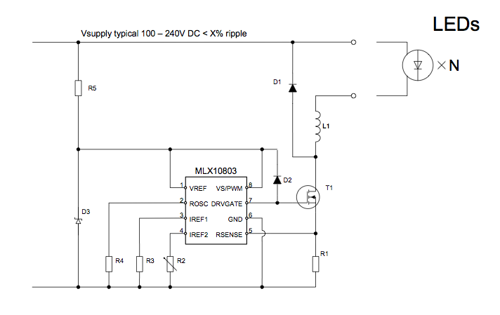
The applications outlined in this document pertain to driving high-power LED diodes. The circuits described can also be utilized in other applications with similar requirements, as long as they adhere to the specifications of the MLX10803. This is a...