
switch mode power supply How does this circuit regulate voltage
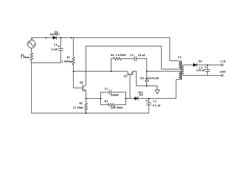
The circuit in question is a modified power supply design based on an old Nokia phone charger. The original charger output of 5.6 V has been adjusted to 12 V through the replacement of the Zener diode, which plays a crucial role in voltage regulation. The Zener diode, when replaced with a higher voltage rating, alters the feedback mechanism within the circuit, affecting the overall operation.
The switching action is primarily managed by two transistors, Q1 and Q2. Q1 is responsible for the primary side switching, while Q2 operates on the secondary side. The upper winding of the transformer (T1) and resistor R5 are integral to controlling the switching of Q1. The half-rectified AC voltage is generated by diode D1 and capacitor C1, which smooths the voltage for further processing.
Q2 monitors the voltage levels on the lower winding of the transformer. When the voltage across D1 drops, indicating that it is no longer conducting, the base current to Q2 is interrupted. This action causes Q2 to turn off, which in turn stops the base current to Q1, effectively disabling it. This feedback loop is essential for maintaining stable output voltage.
The remaining components, C3, R7, C2, R4, C4, and D2, have specific roles in the circuit that may include filtering, stability, and additional voltage regulation. Capacitors C2 and C5 likely serve to smooth out voltage ripples, while resistors R4 and R7 may be involved in setting biasing conditions or providing discharge paths for capacitors. Diode D2 could serve as a protection mechanism or part of the feedback path.
Regarding isolation, T1 does provide some level of isolation, particularly for the secondary winding and components connected to it, such as D3 and C5. This design choice indicates a focus on safety and compliance with electrical standards, even in a cost-sensitive application. The lack of complete isolation for the primary side suggests a compromise in design, prioritizing compactness and efficiency over total electrical isolation.
Understanding the operation of this circuit requires a thorough analysis of each component's role and how they interact with each other, particularly in the feedback and switching dynamics that maintain the desired output voltage.An old Nokia phone charger with 5. 6 V output, so I tried to adjust it to 12 V. By changing the Zener diode though I manged to do that, but I can`t understand its circuit (I replaced the 9v1 with 16v Zener). I would really appreciate any help to understand it. I already understand most of the circuit, but the feedback and switching action isn`t clear. i think Q1 with the upper winding and R5 manage the switching action of the half rectified ac voltage (by D1 and C1). Q2 with the lower winding sense the voltage as when the D1 break conducting current to Q2 base which in turn will open conducting current away from Q1 base so as to turning it off. but what i miss what the remaining components do(C3, R7, C2, R4, C4, D2) Mostfa Mahmod Mar 25 `13 at 7:56 I`m sorry but i cant figure why it isn`t isolated from line voltage i think it is isolated by the means of T1.
and thank you for your time. Mostfa Mahmod Mar 25 `13 at 8:11 According to the schematic, the secondary winding of T1, diode D3 and capacitor C5 are isolated. The rest of the circuit isn`t. Kaz Mar 25 `13 at 8:18 i think because it is a cheap small power supply so it was more cost efficient to isolate the output circuit only not the switching circuit.
however isolation isn`t my concern now as i seek understanding the switching action Mostfa Mahmod Mar 25 `13 at 8:36 🔗 External reference
Related Circuits
This circuit measures the distance covered during a walk. The hardware is housed in a compact box that can be conveniently placed in a pants pocket. The display is designed as follows: the leftmost display, D2 (the most significant...
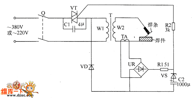
The welder no-load power saver circuit consists of a current detection control circuit and a power saving control circuit, as illustrated in the accompanying chart. The current detection control circuit includes a current transformer (TA), a bridge rectifier (UR),...
An electronic dice is a classic introductory project for individuals interested in electronics. It consists of a timer, counter, and several LEDs, forming a circuit that adds an engaging element to traditional board games. When the switch is activated,...
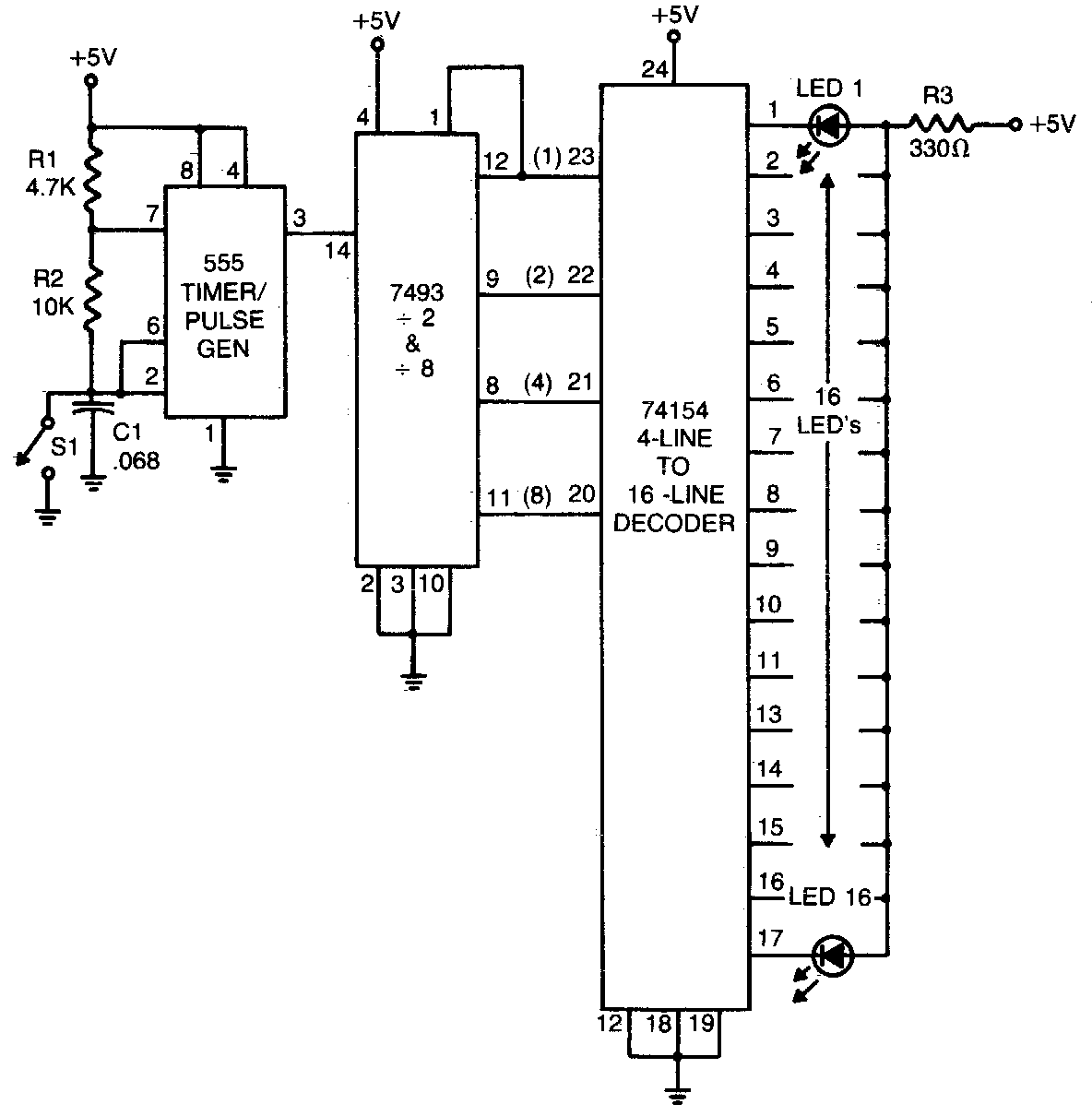
The 555 timer generates a rapid series of pulses when switch SI is open. These pulses are counted in groups of 16 and converted into binary form by the 7493, which is then fed into the 74154, a 1-of-16...
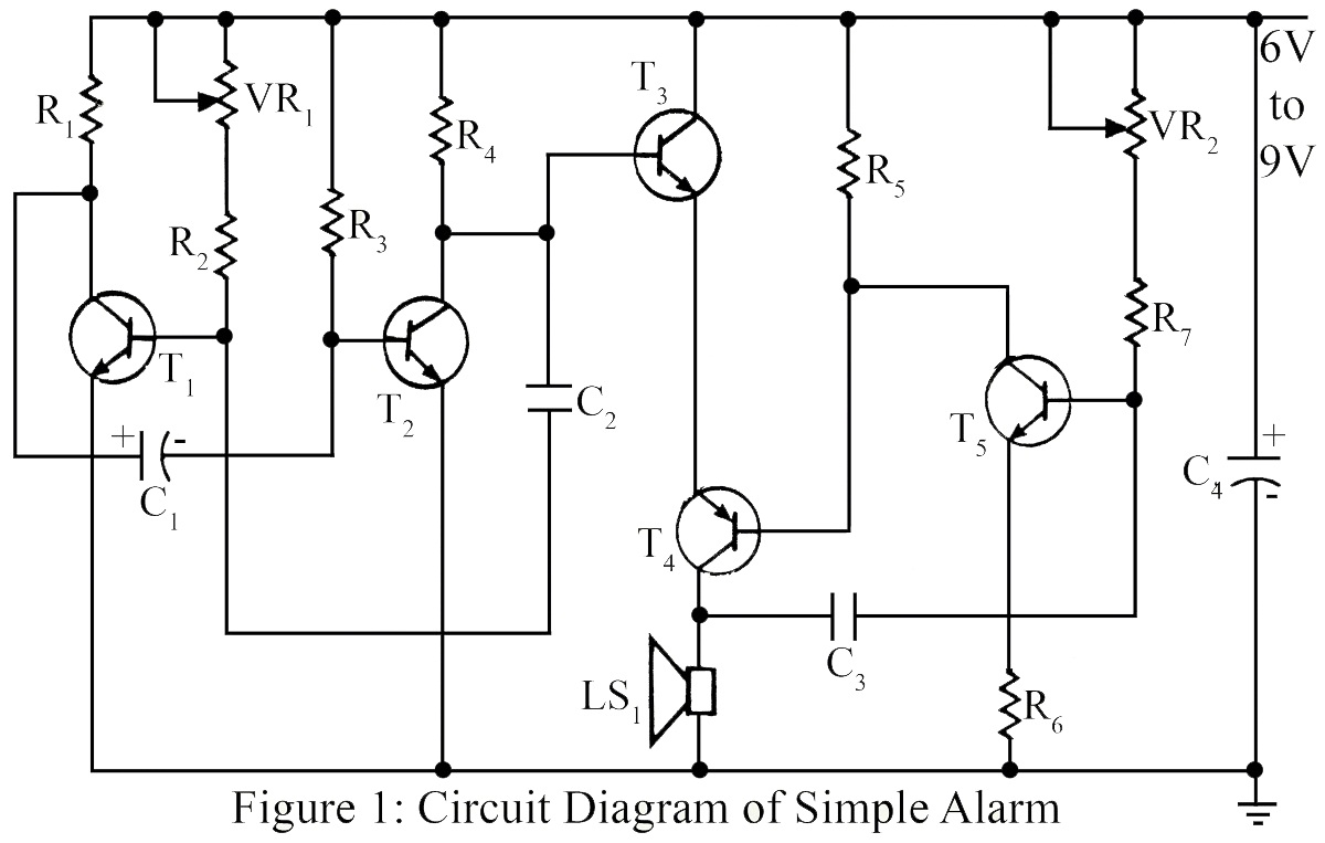
The simple circuit generates an audible alarm notification, functioning as a burglar alarm utilizing five transistors. This circuit operates as a basic burglar alarm system designed to emit an audible sound when triggered. The core component of the circuit is...
The internal disconnection circuit for a blanket operates on the principle of induction. It includes a wire approximately 2 cm in length that senses the proximity of a charged mains power source. When the sensing wire is close to...