
Linear RF Power Meter
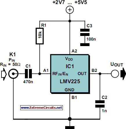
The LMV225 is designed to facilitate precise RF power measurements, making it suitable for applications in various RF and communication systems. The integration of a low-pass filter at the output stage is crucial for minimizing high-frequency noise and ensuring that only the desired modulation components are processed. The ability to switch between active and shutdown modes enhances the versatility of the device, allowing it to conserve power when not in use, which is particularly beneficial in battery-operated devices.
Moreover, the compact SMD package enables easy integration into existing circuit designs without requiring significant board space, making it ideal for modern electronic applications. The specified input impedance of 50 Ω allows for seamless interfacing with standard RF components, ensuring optimal performance in signal detection and measurement tasks. The output characteristics, providing a linear relationship between output voltage and input power, facilitate straightforward interpretation of power levels, aiding in the design and troubleshooting of RF circuits.
Overall, the LMV225 serves as a critical component in RF power measurement applications, with its design tailored to meet the needs of contemporary mobile and wireless communication technologies. The detailed specifications and operational characteristics outlined in the data sheet provide essential guidance for engineers and designers aiming to implement this IC effectively in their projects.The National Semiconductor LMV225 is a linear RF power meter IC in an SMD package. It can be used over the frequency range of 450 MHz to 2000 MHz and requires only four external components. The input coupling capacitor isolates the DC voltage of the IC from the input signal. The 10-k resistor enables or disables the IC according to the DC voltage present at the input pin. If it is higher than 1. 8 V, the detector is enabled and draws a current of around 5 8 mA. If the voltage on pin A1 is less than 0. 8 V, the IC enters the shutdown mode and draws a current of only a few microampG¨res. The LMV225 can be switched between the active and shutdown states using a logic-level signal if the signal is connected to the signal via the 10-kR resistor. The supply voltage, which can lie between +2. 7 V und +5. 5 V, is filtered by a 100nF capacitor that diverts residual RF signals to ground. Finally, there is an output capacitor that forms a low-pass filter in combination with the internal circuitry of the LMV225.
If this capacitor has a value of 1 nF, the corner frequency of this low-pass filter is approximately 8 kHz. The corner frequency can be calculated using the formula fc = 1 G· (2 p COUT Ro) where Ro is the internal output impedance (19.
8 k ). The output low-pass filter determines which AM modulation components are passed by the detector. The output, which has a relatively high impedance, provides an output voltage that is proportional to the signal power, with a slope of 40 mV/dB. The output is 2. 0 V at 9 dBm and 0. 4 V at 40 dBm. A level of 0 dBm corresponds to a power of 1 mW in 50 R. For a sinusoidal wave-form, this is equivalent to an effective voltage of 224 mV. For modulated signals, the relationship between power and voltage is generally different. The table shows several examples of power levels and voltages for sinusoidal signals. The input impedance of the LMV225 detector is around 50 R to provide a good match to the characteristic impedance commonly used in RF circuits.
The data sheet for the LMV225 shows how the 40-dB measurement range can be shifted to a higher power level using a series input resistor. The LMV225 was originally designed for use in mobile telephones, so it comes in a tiny SMD package with dimensions of only around 1 G— 1 mm with four solder bumps (similar to a ball-grid array package).
The connections are labelled A1, A2, B1 and B1, like the elements of a matrix. The corner next to A1 is bevelled. 🔗 External reference
Related Circuits
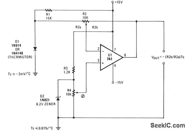
A simple operational amplifier and silicon diode form the core of a temperature-to-voltage converter, allowing the use of a standard voltmeter—either analog or digital—to measure temperature. User adjustments enable readings of either 10 mV or 100 mV to correspond...
What is a circuit breaker? When is an AC power line filter or a phone line filter necessary? How can a noise filter be designed? Is it possible to create a homemade surge protector? The following circuit protection options...
This project has two options. It can be a mains operated project, using a 2155 or 2156 transformer or it can be connected to a plug pack. We recommend it be connected to a 16v AC 1 amp plug...
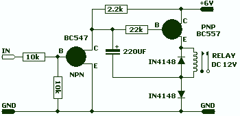
This circuit allows a 12v relay to operate on a 6v or 9v supply. Most 12v relays need about 12v to "pull-in" but will "hold" on about 6v. The 220u charges via the 2k2 and bottom diode. When an...
Chen is in the operational amplifier circuit, utilizing a feedback loop with input resistance that determines the current roll-off. The FET drain current is controlled by the determination circuit, which provides the necessary voltage. The output constitutes a fake...
Many beginners trying out their skill with QRP TX for the first time have to overcome many problems before they are able to come on the air. One usual complaint is that everything is working fine, but the signal...